Preparing for Photonic Integrated Circuit
A gap between the current electronic integration industry and photonic integrated circuit (PIC) technology is present under the subtle tension between “introductory delay” and “collapsing to zero.” Recent standards movement reveals the evidence of this trend through extra-short reach (XSR) definition and points to printed optical board (POB) as the most probable next enabling technology for this ecosystem.
By Kihong (Joshua) Kim and Jeremy Buan, Hirose Electric, Inc. photonic
Photonics has been recognized as a next-generation interconnect solution for electrical systems for many years. However, projected milestones, such as product releases, have been subject to introductory delays. There are two main causes for these delays.
Electrical serializer-deserializer (SerDes) interfaces have led to revolutionary technologies that have extended the use of copper media. However, these developments always drag the photonics debut back to some extent, which we call introductory delay. As an example, SerDes technology is able to compensate for intrinsic material problems, such as dielectric dissipation induced loss, or dissipation factor (Df), and reflection noise through signal conditioners, such as continuous time linear equalizers (CTLE), feed-forward equalizers (FFE), and decision-feedback equalizers (DFE). Other factors, such as mechanical design innovations, also lead to delays. For example, far-end crosstalk (FEXT) is a major cause of suppressed data rates.
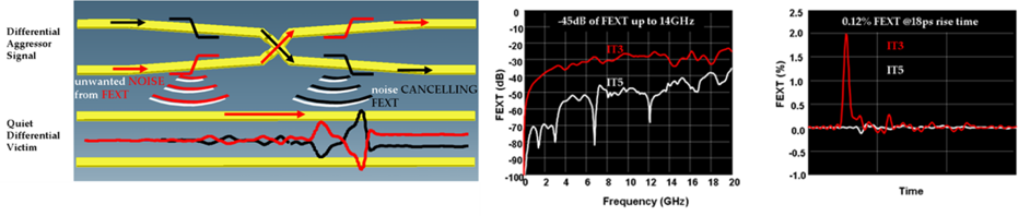
Figure 1: Hirose Electric’s IT8 Series mezzanine connectors use a FEXT-cancellation technology that reduces far-end crosstalk noise by an order of magnitude.
Delays may also occur as the development of related technologies create interference. For example, the incumbent interconnect industry plays an important role in board-level, system-level, and chip-level integration. This technology is solely based on electrical printed circuit board or substrate technology. This domain of technology and its principles are different from photonic integrated circuit (PIC) technology, although PIC technology is also based on Maxwell’s equations. PIC has different boundary conditions imposed on electromagnetic wave solutions: In the electronics domain, two conductors are used to guide electromagnetic waves, whereas interconnection in photonics uses one dielectric material surrounded by another dielectric material to propagate electromagnetic waves. No conductors are involved in photonics, as opposed to multiple conductors in the electronics world. Also, the frequency range that needs to be solved is in the range of a few hundred terahertz for photonics, compared to the range of less than 100GHz for today’s electronics. Another dragging factor is the relatively weaker standards development activities of the photonics industry compared to the electrical society, where standards activities generates an ecosystem of product and application knowledge.
A review of high-speed connectivity from historical and architectural perspectives uncovers some meaningful insights for the connector industry.
Trends in High-Speed Connectivity
As the bit rate of connectivity to carry increases over time, the printed copper trace length decreases. In Figure 2, it appears that this length is collapsing to zero. If this is the case, how can connector companies fill this technical gap?
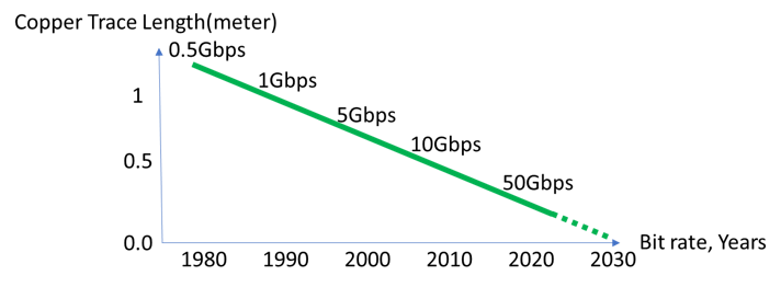
Figure 2: Copper trace length for high-speed connectivity over time
Another trend worth noting is shown in Figure 3, which is projected by the SerDes ecosystem itself. A traditional photonic module, such as small form-factor pluggable (SFP), is an entry point for optics into an electrical system that looks similar to small electrical components. While it is partly geared to the familiar electrical PCB copper trace going to system-on-a-chip (SoC) or integrated circuit, the other half is geared to the optical fiber going to the external world, or out of plane.
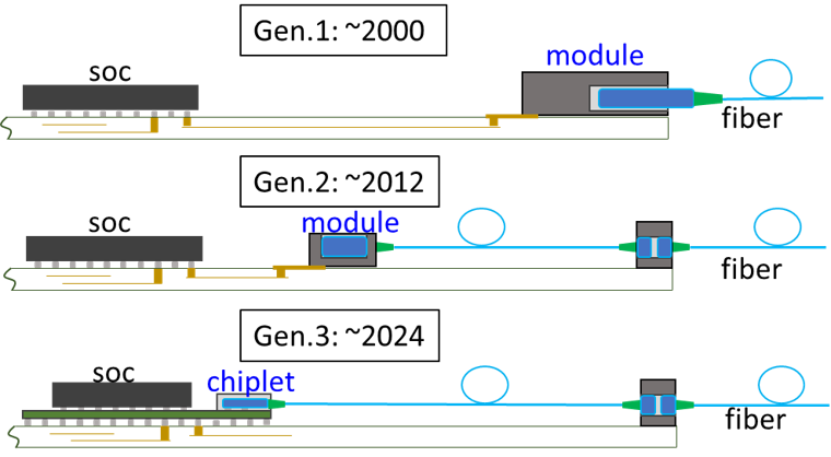
Figure 3: Over time, optical modules have come closer to SoC.
Over the years, the SoC (with SerDes) and the optical module have come closer together. They are merging, as projected by the trend of copper trace collapsing to zero and illustrated in Figure 2).
The Optical Internetworking Forum (OIF) has proposed the use of extra-short reach (XSR) interfaces, in which case the module can be considered to be a chiplet, or a component part of a multi-chip module (MCM). XSR defines the modules that package electronic and optical chips together on MCM substrates. The module I/O of XSR consists of both optical fibers for aggregated data traffic and electrical pads/pins for control and low-speed signal. XSR is a typical example of Gen.3 in Figure 3.
Understanding PIC
Whenever a photonic introductory delay happens, photonic engineers turn their focus deep inside the chip, where less interaction with the electrical world is needed. This causes the photonic circuit to be integrated more and more, to the extent that we sometimes call them silicon photonics (or more broadly termed, photonics integrated circuit). Now, an incumbent electronic integration industry is preparing to learn what comes next with photonic integrated circuit, or PIC.
The PIC concept originated in the 1990s, when the dense wavelength division multiplexing (DWDM) backbone system was developed and deployed for urban infrastructure networks. At that time, engineers suggested a silica-based arrayed waveguide (AWG) filter for the next-gen DWDM system. AWG filters facilitate easy temperature control and are less messy to install. They have served as versatile add-drop multiplexers in urban networks, an alternative solution for incumbent dichroic optical-plate-based DWDM filters, which are bulky and rely on manual assembly to produce and are less reliable for temperature control (Figure 4).
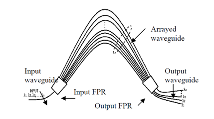
Figure 4: AWG is the first printed optical component on a 2D plane for DWDM systems.
Since then, many more innovative PIC subcircuits, or photonic cells, have been invented, productized, and successfully deployed. A timeline of major PIC subcircuits (green line) is shown in Figure 5. Some of them pre-date the PIC era (blue line) for the telecom market as discrete components. These are integrated directly in PIC or co-packaged as a multichip module.
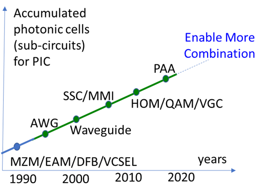
Figure 5: As photonic cells increase, the combinations explode.
Let’s review our common knowledge to prepare for PIC. A laser diode, such as a distributed feedback (DFB) or vertical-cavity surface emitting laser (VCSEL) is the source of a continuous wave (CW) light beam. The light beam is to be further signal processed for its own format through an intensity modulator such as a Mach-Zehnder modulator (MZM) or electro-absorption modulator (EAM) for its amplitude and/or a phase modulator for its carrier phase. Note that the term carrier refers to the real optical carrier of around a few hundreds of terahertz and the term CW emphasizes that fact that the carrier is not yet modulated. A modulated optical signal may go through a waveguide as a PIC internal interconnect to and from each optical functional block (cell), and sometimes further through combiner and/or splitter for fan-in or fan-out purposes. Mode converters (e.g., spot-size converters) are important introductions to fill the gap between sub-micron-sized waveguides and tens-of-macron-sized optical fiber, which is almost two orders of difference larger in size.
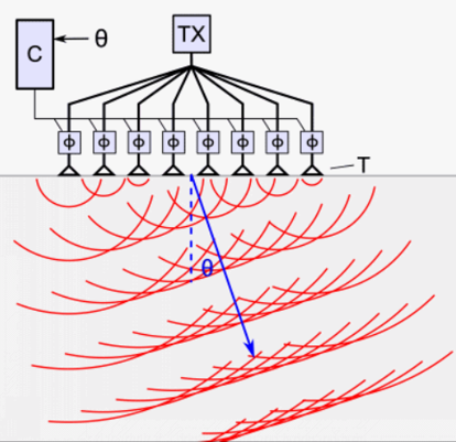
Figure 6: LiDAR (PAA) using photonics cells
It is noteworthy to mention that each cell can work together to create increasingly sophisticated functional blocks. As one representative example, the combination of an intensity modulator and phase modulator can produce a quadrature amplitude modulation (QAM) or higher order modulation (HOM) modulator, as one can imagine architecturally.
Not only does the bandwidth matter, but steering a light beam in free space has been another advanced topic for the automotive market, in which phase-array antenna (PAA) plays an important role in combining these photonics cells (Figure 6).
Off-Chip Optical Bus
As collapsing to zero approaches, one can easily imagine that optical connectors should be crowded in the immediate vicinity of the SoC. Unfortunately, there are no optical I/O standards for this crowded-bus environment. The input and output of PIC (equivalent to the I/O buffer and the bonding pad of the electrical world), which we call off-chip optical bus, don’t seem to have any candidate solutions, industry consensus, or standard activities. This is an obvious and immediate problem and a near-term challenge facing connector companies that are involved with PIC components.
The two major off-chip interconnection types of PIC are (1) direct coupling to vertical grating coupler (VGC), as shown in Figure 7, and (2) traditional edge (butt) coupling with spot-size converter (related simulation shown in Figure 8). The first approach provides fiber coupling from surface grating of PIC. Although it has limited bandwidth, more coupling loss, and polarization dependent loss (PDL), it gains more consensus when volume production matters. The second approach generally provides very low PDL and coupling loss. However, selecting a known good die is impossible before dicing wafers when processing for PIC.
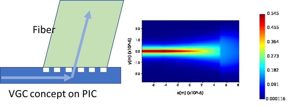
Figure 7 (left): VGC on PIC coupling to fiber. Figure 8 (right): Spot-size converter simulation example (using Lumerical’s MODE simulator).
Note that for both cases, fiber is the one that directly couples to and from PIC. This is because of the lack of intermediate technology available, although some companies are dedicated to its promotion (e.g., by using electro-optical circuit boards [EOCB]) [1]. Some companies promote optical interconnections embedded in conventional PCBs.
Introduction of the Printed Optical Board (POB) to the Electrical Ecosystem
As mentioned in the previous section, overcrowded optical connectivity near the vicinity of the SoC is an immediate tough problem. The simple answer for such connectivity crowdedness could be realized by a provision of a mitigation stage in terms of physical dimensions. Suppose we have a PIC and multiple fiber connector to be connected from the SoC to typical optical connectors such as multi-fiber pull-in/pull-out (MPO) and standard connectors (SC). One possible answer is to fan-in/fan-out with the given number of connectors. Using current technologies, such as MPO [2] or SC, it is obvious we will see bulky fiber bundles and mechanical fiber enclosures.
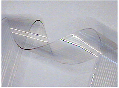
Figure 9: A polymer waveguide example from ChemOptics.
We would like to propose an intermediate solution, polymer waveguide (Figure 9) [3,4], to mitigate issues with the existing interconnection technologies. Assembled with connectors that are compliant to a certain specification, as seen in Figure 10(a), we call this board a printed optical board (POB). POB helps create smooth transitions from the micro PIC world to the macro fiber world.
A polymer waveguide film is very similar to an electrical PCB in that it carries signals and can be patterned on a two-dimensional plane. It can be 2.5-dimensional through optical via structures. It can also be physically overlaid on existing electrical PCBs to provide alternate high-speed paths to prepare for the zero collapsing shown in Figure 10(a). However, it differs from PCB in the sense that it carries optical signals rather than electrical signals. As such, connectors and waveguides need to be analyzed through the governing Maxwell’s equations in principle at the frequency range of a few hundred terahertz using a different algorithm, mostly for fundamental transverse electromagnetic (TEM) mode in a hetero-dielectric system without any metal boundary. EDA tools, such as Lumerical [5], are readily available to design and simulate such interconnects.

Figure 10: POB types (a) overlaid POB on PCB (b) optical waveguide is embedded. Green lines depict the light paths.
Figure 10 shows two types of POB: (a) the method that is more likely to be productized in nearer future and (b) existing proposals from some companies [1,6]. The optical layer pictured in Figure 10(a) is processed separately and overlaid on pre-processed PCB when assembled. This requires precision processing to align PIC (optical chip) to POB and POB to PCB. However, PCBs and POBs have their own fully matured, reliable, and cost-effective manufacturing processes. The optical waveguide core layer pictured in Figure 10(b) is embedded in a PCB material and process. Since the optical layer and the electrical layer are aligned in manufacturing, assembly houses do not need to provide extra alignment. However, the material system requires a new lamination process, which increases the cost and yields unknown field product reliability.
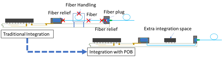
Figure 11: POB provides cost reduction and reliability enhancement as an intermediate interconnection solution for PIC.
The most prominent benefit is cost savings. The cross marks in Figure 11 indicate each point where one can expect to reduce the components required, such as fiber relief and fiber handling mechanical enclosures with stand-offs where extra space is needed. It is noteworthy that dangling fiber can create another source of coherent noise. Therefore, optical interconnect on a fixed film or board provides more stability from vibration and temperature gradient, which is amplified when the bandwidth increases. Likewise, it increases manufacturing reliability through the reduction of several manual assembly points, which will consequently reduce the overall cost.
Type A POB Application
Figure 12 shows details about the connector placements. At position 1 (P1), where a bare die (PIC) to package I/O should meet and is expected to be well coupled for an optical signal, the P1 connector should be newly defined and specified in terms of mode and intensity coupling for both sides of the interface (e.g., PIC on one side and POB waveguide on the other side). Considering PIC interfaces are commonly designed for single-mode fiber (SMF), the P1 connector should be focused on POB waveguide coupling efficiency, assuming that SMF interface technology is readily available.
At P2, half of its interface is already defined with the de facto SMF and multi-mode fiber (MMF) standard. The SMF interface is expected to come to market first, due to the high demand for high-end systems for data centers, etc. Therefore, P2 connectors need to focus on POB waveguide mode with reasonable mechanical alignment, assuming that SMF interface technology is readily available.
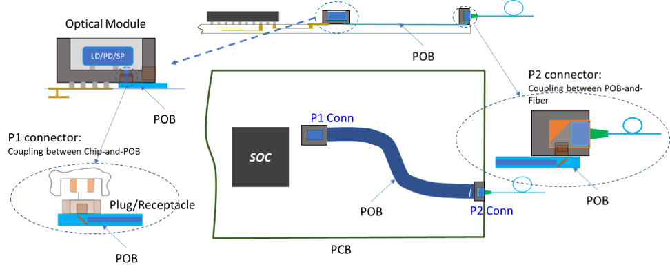
Figure 12: POB application in Gen2 integration example.
Conclusion
We reviewed the integration aspect of silicon photonics, or PIC, for the remaining electronic system. We found that a gap between the current electronic integration industry and PIC technology is present under the subtle tension between introductory delay and collapsing to zero. However, recent standard movement, such as OIF, reveals the evidence of a collapsing to zero trend through the XSR definition. Reflecting on these changes in the field, we believe the most probable next enabling technology for the ecosystem is POB to prepare an economical and reliable solution for the post-collapsing-to-zero era. Type A POB connectors are reviewed and explained from an architectural perspective. PIC-to-POB and POB-to-PCB alignment technology should be a key development target. Both P1 connector and P2 connectors require efficient fundamental mode coupling between POB waveguide and SMF (or its equivalent). Further research is recommended to optimize POB waveguides for SMF (or SMF-like) interfaces in conjunction with state-of-the-art SerDes channel configurations.