Signal Integrity is Key to Today’s High-Speed Connectivity Designs
Learn how to design systems that minimize signal integrity loss and interference and maximize performance.

The bar is higher than ever for high-speed performance, and PCB components have the potential to be either a great asset or an Achilles’ heel, especially if signal integrity is not given the foremost consideration while testing the design. What was previously only a problem for high-frequency applications is now encountered by hardware developers across the digital sphere due to the demanding nature of high data rates, some even exceeding 20+ Gb/s. Even in low-end applications, demand is increasing for smaller, faster, and more capable electrical components while less and less space is available on the rapidly shrinking real estate available on today’s PCBs.
Basic design requirements are always in play: how much space is available on the module, floating capability, the desired connection technology, the number of pins and the pin assignment, as well as overall performance requirements. The most pressing challenge is to manage these requirements successfully while avoiding the looming threat of signal loss during module operation. If the present signal paths are dampened or lost, the multitudes of additional design factors can become entirely irrelevant as the components lose their ability to transmit data. For a module to work at peak operational capability, defending against signal loss must be at the forefront of design.
Defending Against Signal Integrity Loss
The types of materials present near the signal path are critical to the success of a high-speed signal. It is important to avoid cross-sectional changes in the contact material and to use material with high conductivity. The dielectric constant of the plastic material also affects signal transmission. The typical standard for phase matching throughout an interconnecting system is 85-100 ohms.
Because electronic components can act both as an interference sink and as a source of interference, the proximity of sensitive components increases the risk of mutual interference. A high-speed signal can be lost through insertion loss as well as return loss. Insertion loss is the deviation(s) within the impedance curve, resulting in signal reflections. This describes the loss of a signal along the signal’s path, presented as the ratio of outgoing to incoming signal. With a high insertion loss, a signal can no longer be clearly identified by the receiver and therefore a limit value of -3 db is typically set.
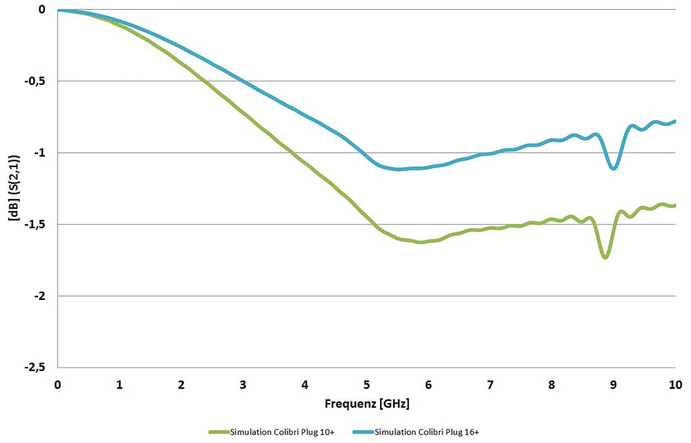
Figure 1. Optimization of the ept Colibri connectors from 10+ Gb/s to 16+ Gb/s. Graphic: ept GmbH
Insertion loss is made up of different components: coupling losses, dielectric losses, reflection losses, line losses, and radiation losses. Coupling losses occur at the contact point between the male and female connectors. Reliable contacting with appropriate tolerances when plugged in is crucial to reducing signal transmission losses. The ohmic contact resistance should also be kept as low as possible through a large contact area and a high contact force at the contact point. Foreign materials on the connector surface, such as particles produced by abrasion, can increase the contact resistance. High-quality connectors are provided with at least a superficial layer of gold to prevent this from occurring.
Apart from the insertion loss, the return loss must also be considered. Return loss is the portion of the reflected signal in the inserted signal. Given a connector’s impedance profile, there is little room for a system designer to further influence the return loss. The best way to do this is with the rise time or the pinout. The rise time describes the time in which the signal lies between two defined amplitude values (typically between 10% and 90%). The lower the rise time, the greater the bandwidth and the closer the impedance is to that of the rest of the system.
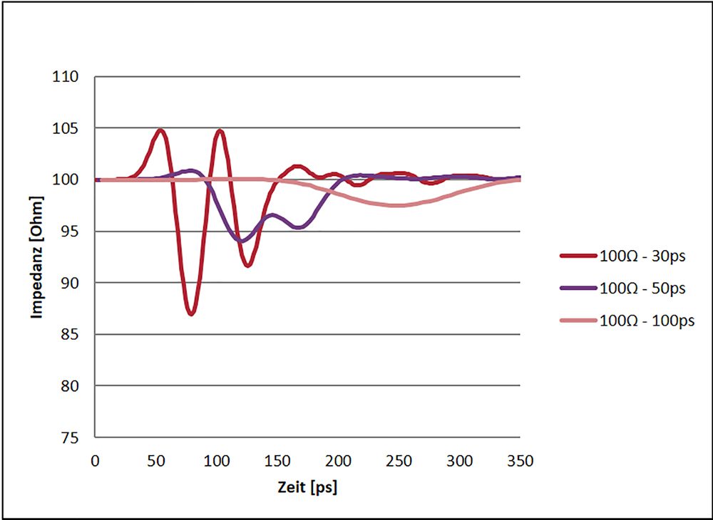
Figure 2. Dependence of the impedance on the rise time. Graphic: ept GmbH.
Another critical source of signal interference is crosstalk, or the undesired influence of a differential signal by another signal on a different line. The capacitive and the inductive coupling can be considered separately. Near-end crosstalk (NEXT) occurs when the signal transmission of a pair interferes with the signal transmission of a parallel pair, which mainly occurs through induction. The higher the frequency, generally the more interference will affect the second pair. If the absolute value in decibels is high, there is a high level of crosstalk attenuation, so only a small influence can be measured in the disturbed pair. At a value of -20 dB 1% of the signal crosstalk. At a value of -40 db, on the other hand, only 0.01%.
In contrast to near end crosstalk, far end crosstalk (FEXT) occurs over the entire length of a line. Interference with the signal from a neighboring pair is therefore measured at the end of the transmission link and is usually lower because the interfering signal is attenuated along the line.
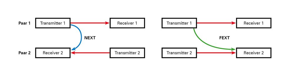
Figure 3. The effect of near and far crosstalk on signal transmission. Graphic: ept GmbH.
Crosstalk can be reduced by layouts in the pinout by placing two potentially influencing contact pairs away from each other with ground contacts. A contact design with the shortest possible signal paths also reduces the influence of crosstalk.
Of course, data transmission within a PCB system must not be disrupted, falsified, or prevented, which is why protection from electromagnetic interference is a topic of great concern for signal integrity in high-speed systems. Electromagnetic interference can be comparable to crosstalk; the only difference is that the source of interference is not within the individual signal paths in the connector but is produced externally.
High-speed data transmissions are particularly susceptible to interference from unwanted electromagnetic effects; even a small impulse can falsify a useful signal and prevent the receiver from clearly interpreting the digital information.
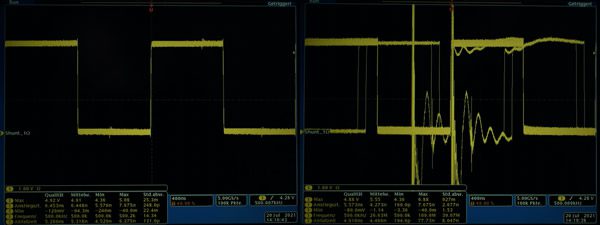
Figure 4. Interference of the useful signal with the shielded (left) and unshielded (right) connector. Graphic: ept GmbH.
A connector can represent both an interference sink and an interference source; it can be influenced by other components of the assembly and have an electromagnetic effect on surrounding components. With the coupling inductance LK, the connector can be described in both functions – as source and sink.
The coupling inductance is to be regarded as an EMC parameter since the connector can be easily described by considering the electrical conditions. This applies to interference immunity as well as interference emission. The coupling inductance is not a measure that applies equally to the entire connector because it can be influenced by the signal assignment on the connector and the connector geometry.
Example:
As a case-specific example, a maximum coupling inductance of 47 picohenry (pH) was determined for an HDMI signal at a voltage of 4.4 kV. Comparatively, coupling inductance values are between 1 and 4 pH. with the shielded connector.
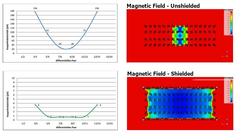
Figure 5. Simulation of an unshielded (above) and a shielded (below) connector. Graphic: ept GmbH.
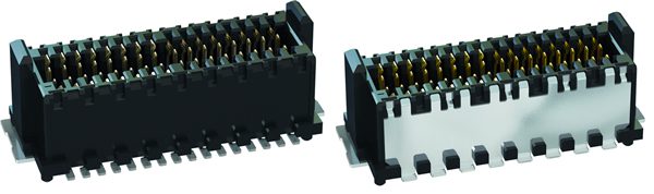
Figure 6. Example of a 0.8 mm connector in its unshielded (left) and shielded (right) versions. Graphic: ept GmbH
A prerequisite for effective shielding is to use a material with high conductivity. The number of contact points can be decisive for successful shielding. The interference current induced in the shield of the connector in turn generates a magnetic field that can affect the signal contacts. The higher the current, the stronger the magnetic field. The current flow is divided by multiple contacting of the shielding plate and the magnetic field is thus reduced.
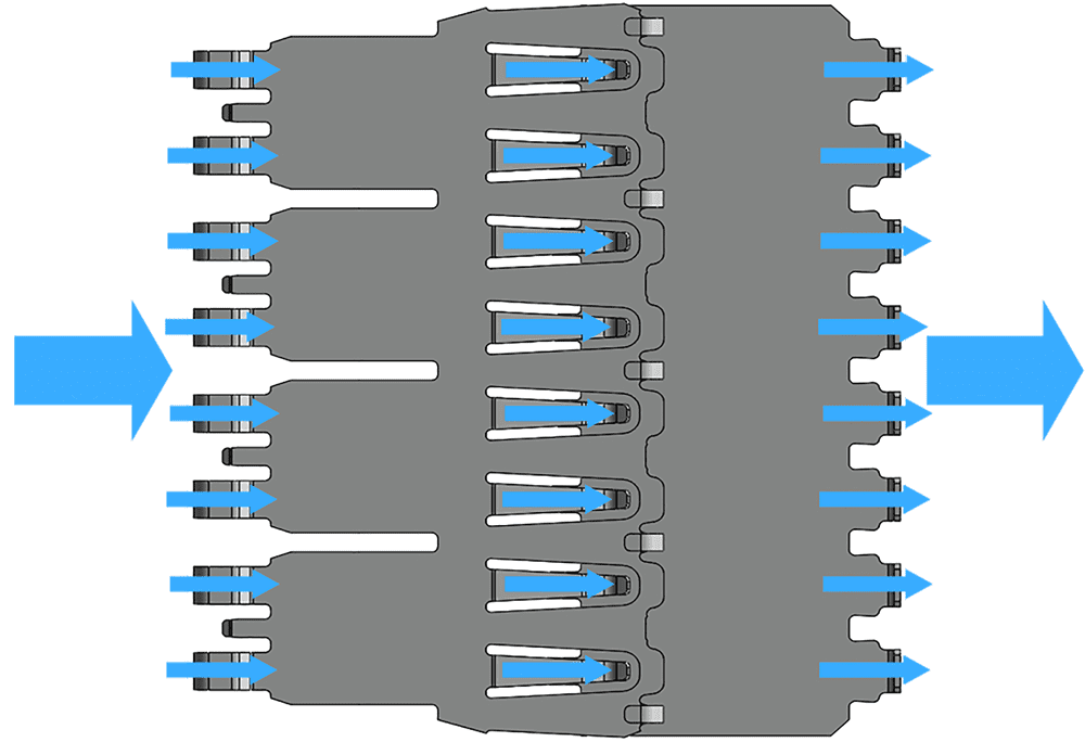
Figure 7. Distribution of current flow through a shield plate. Graphic: ept GmbH
The risk of signal loss increases as the need for high-speed connectivity surges. The higher the frequency of the signal, the more difficult it is for the recipient to understand the sender. The goal when developing new high-speed connectors is to minimize this interference within the transmission path. Careful consideration of materials, the possibility of EMC shielding, insertion loss, return loss, and crosstalk is essential to optimizing high-speed design potential.
Visit ept Connectors to learn more about solutions to maximize signal integrity.
Subscribe to our weekly e-newsletters, follow us on LinkedIn, Twitter, and Facebook, and check out our eBook archives for more applicable, expert-informed connectivity content.
- Signal Integrity is Key to Today’s High-Speed Connectivity Designs - November 1, 2022