Test and Burn-In Sockets: The iNEMI Roadmap
Test and Burn-In Sockets: The iNEMI Roadmap
 Test & burn-in (TBI) sockets represent a small but technically challenging segment of the connector industry. Designs are robust, leading-edge, often produced in small quantities at very high costs, and are tested in excess of 100,000 touchdowns before socket rebuild. The market segment focuses primarily on the IC industry, and system prototyping, emulation, and test. Singulated and strip test sockets and burn-in sockets are considered part of the electronic connector market, while wafer probes are designed to test bare die and wafers in the semiconductor equipment market.
Many TBI sockets are closely linked to silicon packaging and Si technology trends, including some of the most demanding requirements in the connector industry:
- Highest speed
- Highest density
- Lowest voltages and noise margins
- Rigors of high-temperature burn-in tests
- Impact of Moore’s Law on discrete interconnect devices
- Backdraft from increasing IC test costs
- Threats from wafer level/flip chip, MEMS, 3D, and other die-level test technologies
Thus, test socket manufacturers tend to be a separate breed from production connector manufacturers. Their business postures involve high levels of engineering, low-volume/high-tech manufacturing, and (typically) a different set of customers.
Critical Issues:
- Semiconductor performance — electrical, mechanical, and density — continues to increase and is approaching the limits of conventional socket technology, although recent slowing of Moore’s Law indicates showstoppers may be further in the future than originally thought.
- Semiconductor test costs are a critical issue for the semiconductor industry. This places pressure on the test supply chain and will result in new test & burn-in strategies, such as combining TBI and wafer-scale tests.
- IC packaging is changing, albeit slowly, toward flip chip and 3D chip packaging. Conventional sockets typically do not test unpackaged ICs (pad density). This requires probe testing, with pad pitches below discrete socket capabilities.
- Test socket makers continually face new challenges, which are overcome each year with few, if any, roadblocks.
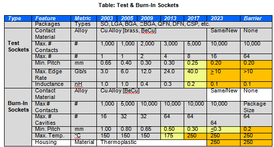
Test Socket Technology Trends
Key technologies for test sockets include:
- Contact design for socketing of IC packages exceeding 10,000 touchdowns
- Contact design for fine-pitch applications ≤ 300 microns
- Engineered housing materials and design for rigorous test environments
- Electrical modeling and simulation at very high multi-GHz performance levels
Test sockets are used for package and die verification, device characterization, failure analysis, and debugging. Once the package and/or device are characterized, the OEM generates a final test program to use with the test socket/contactor during large-volume, final testing.
A key component of test sockets is long insertion life without contact degradation. Not all devices require such high performance, though. In some cases, production or B/I sockets can be used as test sockets because the devices are inexpensive. In general, a long-life, high-performance test socket will cost at least 10 times more than a B/I socket and deliver 300-500K insertions before rebuild.
Key Design Issues
The key design issues for high performance test connectors are increasingly lower voltages and faster edge rates. At lower voltages, connectors are getting noisier by comparison, with higher crosstalk. With microprocessors dropping below 2 volts, required performance is now in what was considered threshold noise level only a few years ago. With 5V TTL logic and 20-80% as the unknown state, there used to be a low-end level of ~1V. Today 1V is very close to the high end.
Thus, the noise ceiling of a few years ago is today’s logic 1 floor. Edge rates are getting faster with tighter timing window requirements. Even if a part only runs at 250MHz, edge rates are important, because that part may be syncing with another running at 3GHz. Thus, when the part is clocked it has to change state as though it were a 3GHz part. If it didn’t, it would miss the time window or cause a latent state, as it took two to three clock cycles to change state. This requires connectors that do not delay or distort the signal, especially in test applications. Crosstalk is one of the bigger issues. It appears the answer is LVDS (low voltage differential signaling).
There is also a need for lower-force connectors that do not crack thinner die. This is especially true of large devices, which include BGA, LGA, etc. The die is made thinner to increase performance and reduce cost, but the pin count is rising, at up to 10,000 I/O on the roadmap for some server ASICs and CPUs.
Consider how many discrete devices were once used to assemble a PC board. Over time, these functions were integrated into a single die. Now IC manufacturers are beginning to use different fabrication techniques on the same die (e.g. multi-core, logic, and memory). As functions are integrated, there is increased demand for higher frequency sockets to test larger BGA packages. This is because they have integrated SERDES (Serializer/De-Serializer) circuits into low frequency devices such as FPGAs. In addition, bus structures are now high-speed serial versus parallel, all leading to higher-speed socket requirements.
Key Points
Falling voltages, quicker edges, higher frequencies, smaller pitches, and higher densities are all pushing for higher-fidelity sockets in smaller footprints, a continuing challenge for test socket makers.
Other considerations include:
- Increase in strip testing, mainly for lower-speed mixed signal small QFN and SO-type devices; strip applications are dominated by Pogo pin solutions and need to withstand up to a million touchdowns
- Finding contact probe metals that will handle continuous solder contacting (solder balls); designers are now looking at lead-free options
- Pad wear-out: NiPd pads are wearing out contact pins down to
- Intermetallic is an issue, if not a roadblock.
- Solder build-up increases contact resistance (although there are ways to compensate for CRES), and the issue isn’t CRES. It is variation in CRES, with some contacting technologies much better at maintaining a constant CRES. This changes DC and AC parametrics and also increases yield fallout. (Some current solutions require frequent changes to the test probe, which increase retest costs and the overall cost of testing. Some technologies do well with cleaning cycles; some have inherent CRES issues in the contact design.)
- Burn-in: The biggest issue appears to be pitches below 40 mils (1,000 microns), especially in memory devices, as well as diminishing ball size on CSP devices. The package is moving closer and closer to the wafer, either flip chip or chip scale.
Major Roadblocks
Major roadblocks in the TBI area include the following (plus an estimate – in parentheses – of when that roadblock has occurred or will):
Test
- Multiple package test (began in 2001) significantly changes single package test & burn-in socket design. Multiple package testing has been happening for quite some time. Tester resources and cost have limited this trend. A requirement for higher speeds on more pins simultaneously is a limitation. Improvements are steady year to year. A bigger issue is the cost of testers. There are no real roadblocks, just a consistent progression. A big issue in memory is 128 moving to 256 devices in one insertion; tri-quad and possibly octal has moved to higher-end analog and RF testing and has already moved to strip testing on low-cost parts.
-

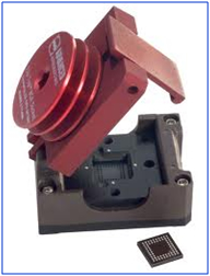
Wafer test, Cascade Microtech
Wafer scale test (began in 2006) reduces or eliminates the need for package testing. The requirement for a membrane-type vertical socket that can handle high frequency, high density, and high touchdown counts is still in the future. Developments in process will be more evolutionary than revolutionary. Keeping the cost-per-pin to a reasonable level for probe cards and probe stations, and being able to replace pins at a reasonable cost, is where the industry needs to be. This requires significant R&D costs with unsure returns.
- Pad pitches for wafer scale test (began in 2004): Pitches in the 4-6 mil range in bare-die testing (i.e. wafer probes) will require new technology. These include micro spring/MEMS-type contacts and PTFE/Elastomeric interposers, which are all new technologies to connectors.
Burn-In
- Reduction/elimination of burn-in due to cost pressures (began in 2000): This has already begun in some memory devices (Flash) and is expected to increase; combined test/burn-in is now in use.
- No roadblocks but costly solutions: High pin count BGAs have sensitive die limiting contact force on the die, and the devices also require cooling during TBI. This increases costs in startup and operations. Reducing the force/pin on high pin count devices is also critical to reducing overall package forces. These are critical issues because the package and the die are getting much more sensitive to external forces as they get thinner to support higher speeds and faster thermal dissipation.
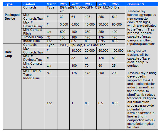
Test-in-Tray
There is a growing consensus that TBI requires a new approach. SEMI’s CAST consortium is the latest effort to bring focus to an aspect of this looming problem. TBI consumes an increasing portion of the manufacturing cost of semiconductor devices (up to 20% in some cases). The problem continues to worsen as test time grows with increasing device complexity.
 Test-in-Tray technology has the potential to greatly reduce the cost of TBI, initially by enabling parallel test of trays of devices with rapid index times. Only ATE resources limit parallel test. Test-in-tray has the potential to reduce escalating test costs, particularly with new wafer scale packaging, CSP, and flip chip devices. Adoption is slowed by sunk costs in legacy equipment and by risk-adverse contract test houses. The test-in-tray approach provides the test efficiency of strip test without limitations on device types. Trays can handle all package and device types, from large BGA/LGA packages to WLP and bare die formats, all with the same automation transport standards.
Initial adoption of test-in-tray methods has been in MEMS and automotive electronics, which require extensive testing. As alignment accuracies improve, WLP and other fine pitch devices will be tested in trays that allow automated burn-in and test sequences in a more cost-effective format than with probe cards on wafers. Testing trays of mostly good devices allows more effective use of ATE resources than testing un-yielded wafers. Bare dice are transported with a minimum of human intervention.
With full test-in-tray automation, devices remain in a tray throughout back-end processing, including all test and burn-in steps, speed sort, trim, post-processing, mark, and packing.
Test-in-Tray Automation
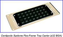
Participants in the iNEMI Roadmap process contributed to this article, in particular Dr. Thomas DeStefano, founder of Centipede Systems.
- Electric Vehicles Move into the Mainstream with New EV Battery Technologies - September 7, 2021
- The Dynamic Server Market Reflects Ongoing Innovation in Computing - June 1, 2021
- The Electronics Industry Starts to Ease Out of China - November 3, 2020