Great Connector Inventions: Compliant Press-Fit Pins
Compliant press-fit pins are a key achievement in the development of backplane connector technology. Here’s how they work.
Compliant pins, waferized connector designs, modular connectors, egg-crate shielding, air-dielectric designs – we can now look back on inventions like these and put them in perspective. It is interesting to see how a real understanding of the technology and the problem, as well as a vision toward the future, can lead connector design engineers, and now signal integrity engineers, to outside-the-box solutions that fundamentally improve connectors and change the industry in the process.
One of the most fundamental connector technologies, compliant press-fit, did not exist until the 1970s when Robert Knowles of Winchester invented the C-Press compliant pin and convinced Western Electric, the manufacturing arm for the AT&T monopoly, to qualify this new technology. Up until then, backplane pins were either soldered or rigid square or rectangular pins were forced into plated through-holes. For this process to create a gas-tight joint, the hole tolerance had to be +/- 0.002″ (5%), which was very challenging, especially for large boards. The dominant technology at that time used large 0.040″-diameter holes with 0.025″ square pins.
The telecom companies designed nearly all of their equipment for 25- to 40-year lifespans. That sounds like a lot until you realize that the junction box on your street corner is quite likely to be that old. We are always adding capacity to networks, but if the old lines still work, they remain in place. Today, that model has been overturned by the internet, massive data-center-centric networks, wireless, and ubiquitous video.
Anyway, back to the importance of compliant pins. The C-Press pin was fantastic in service, but difficult to stamp. This pin contacted >70% of the diameter of the plated through-hole. The conservative operating companies tested these compliant pins through accelerated life testing to ensure they could last for 40 years. They learned that electrical performance was comparable to soldered pins and the compliance made these much easier to use in manufacturing, opening up PCB hole tolerances to +/- 0.003″ (7.5%). The effect of this was profound:
- PCB prices came down because they could be drilled at faster speeds with fewer drill replacements.
- Thicker boards were much more practical and allowed for higher layer counts, more density, and more power.
- Press-fit pins are now repairable, even in the field. (Imagine trying to remove and replace a broken soldered pin.)
- Pin-stitching or mass insertion processes allowed for custom configuration as the backplane was made. Frequently the header shrouds were then placed over the pin field.
- Pins could be left out, allowing OEMs to only pay for the pins they needed.
- Multiple pin lengths were possible, facilitating sequenced mating, an important enabler for hot swapping of cards.
OEMs would often use wire wrapping for small-volume production, common for prototyping and development. Keep in mind that CAD was just coming into use and much of the PCB layout was still done by hand, and therefore was expensive, error-prone, and extremely time-consuming. Wire wrap allowed simple machines to place wires to connect pins. Press-fit pins with no solder were very friendly to this process.
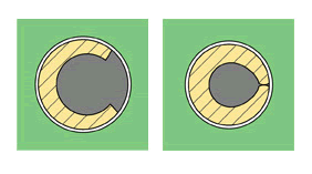
Cross-section through the C-pin-compliant section in the largest and smallest holes
The C-pin was the first broadly used design, but over the years, the eye-of-the-needle (EON) design has proved to be the most adaptable and durable design, especially as the contact pins and plated through-holes shrank. Compliant pins are now used in holes as small as 0.012″ in diameter.
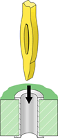
Eye-of-the-needle compliant Pin (illustration from Cleaver Brinkerhoff)
Nearly all of the fine-pitch compliant pins use the EON. The earliest patents for EON pins are from William Robert Evans, then with AMP in Harrisburg, Pa, and Len Johnson and Roy Barnett of Teradyne. Initial designs used a pin that was nearly the size of the hole with a rectangular cross section. Later, improvements coined the portion of the pin that mates with the hole, which reduced insertion forces and protected the hole plating. Further improvements involved refinements to the outer surfaces, as well as refinements to the shape and position of the hole. Woody Wurster of Custom Stamping has tooled EON pins for every conceivable form factor, including backplane and edge-card connectors. Wurster also has EON patents for enhancements to the EON shape and has provided pins for many of the top connector companies over the years.
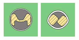
Molex M-Pin and TE Connectivity Action Pin are examples of compliant sections.
To get around these patents, other connector companies quickly designed a number of competing designs that used different shapes of the compliant zones to achieve a gas-tight joint. AMP, now TE Connectivity, invented the Action Pin that it still uses today. Other shapes like V-press, sigma pin, and tri pin proliferated quickly.
When the EON patent ran out in 1991, all vendors were free to adopt and tool the EON pin that is the dominant design today.