Top 12 Technology Trends: The Amazing Shrinking Chip
After more than 50 years of miniaturization, the transistor and Moore’s Law may be nearing their technical and economic limits. However, new innovations in silicon photonics promise to extend the evolutionary timeline into the future.

This is the eleventh in a series of articles that review leading technology trends that have had a significant impact on the electronic connector industry.

The Amazing Shrinking Transistor
The creation of the first transistor in 1947 sparked an evolutionary spiral that has forever changed our world. The technology evolved from a single gate on a chunk of germanium when engineers found ways to fabricate multiple devices on a common silicone substrate. Introduction of commercial transistor radios in the mid-1950s was a harbinger of how this new disruptive technology would alter expectations for electronic devices. No longer hobbled by the large size, excessive power use, and heat of a vacuum tube, electronic products could become smaller, lighter, and more energy efficient, eventually enabling powerful laptop computers and an entirely new class of mobile devices. Eighteen years later, Gordon Moore suggested that the number of transistors on a chip would double about every two years, a prediction that held true for over 60 years.
The Integrated Circuit
The development of the integrated circuit in 1961 allowed the fabrication of multiple types of semiconductor devices, including memory and passive components on a single die, to create complex functional circuits. Advanced photolithography and deposition processes produced ever smaller devices on denser centerlines.
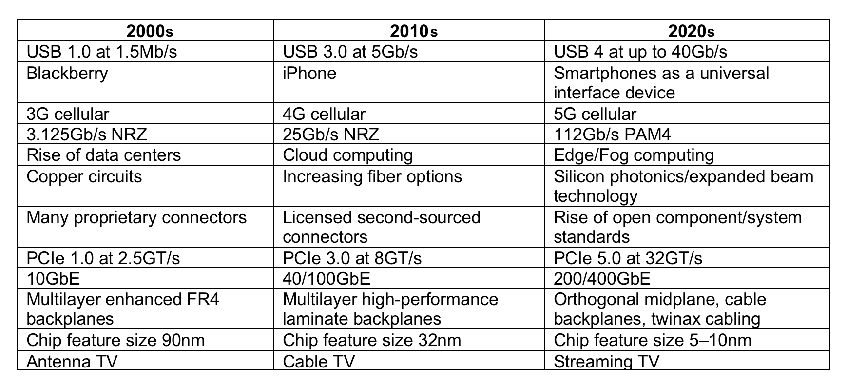
Placing active devices in proximity increases the number of devices per chip and wafer and allows greater device functionality while reducing the cost per chip. Shorter links between devices reduces latency, allowing faster performance. Demand for more powerful computing capability in smaller envelopes touched off a race to shrink the transistor to near atomic levels. The scaling of fabrication processes resulted in a continuous cycle of squeezing more transistors onto a monolithic die. The first multi-core processor chip was introduced by IBM in 2001 and was designed to simultaneously manage multiple processes more efficiently while consuming less power. With features measured in nanometers, the industry had achieved high volume production capability of devices, with 32 nm nodes by the late 2000s. Additional architectures, including the development of the microprocessor, microcontroller, system-on-chip (SOC), and the three-dimensional IC, enabled entirely new segments of the industry to flourish. The result of these remarkable advances in device fabrication accelerated the ongoing revolution of electronic devices that pervades every aspect of our lives today.
After more than 50 years of miniaturization, the transistor and Moore’s Law may be nearing their technical and economic limits. As devices become more tightly packed, accumulating heat can build up to exceed maximum temperature specifications. Insulation between elements becomes so thin that current leakage becomes a problem. The wavelength of light used in the photolithography process is reaching limitations to create finer features. The decline in the curve of transistor dimensions has begun to flatten out although engineers continue to find ways to increase the transistor count per die through advanced manufacturing processes, including the use of extreme ultraviolet imaging technology.
Improvements in semiconductor processes continued to advance with transistor dimensions shrinking from 32 nm, 22 nm, and 14 nm. In 2017, Intel announced that it can pack more than 100 million transistors in each square millimeter of chip using its 10 nm technology. The same year, IBM announced a new 5 nm process that would enable placement of up to 30 billion transistors on a chip the size of a human fingernail. Recent chip designs are being customized to support specific features or applications. Nvidia recently announced its Grace CPU, which is optimized for artificial intelligence calculations. Korean company Zinitex is developing an AI chip, designed for intelligent TV and voice recognition applications, that processes data at 40 trillion cycles per second and consumes minimal power.
New Chip Fab Plant in Arizona
The cost of building and equipping a state-of-the-art chip fab plant runs into the billions and takes years to become operational. Very few companies can support that level of long-term investment. TSMC’s 5 nm technology will be utilized in a new facility slated to begin construction in Arizona. It is scheduled to produce 20,000 wafers per month by 2024. In addition, 4 nm, 3 nm, and 2 nm processes are in development. TSMC has budgeted $100 billion for R&D and fab construction over the next three years.
Research is underway to determine if it is physically possible and economically feasible to fabricate transistors by manipulation of individual atoms. The recently passed American Jobs Plan infrastructure bill includes earmarks of $50 billion for advanced semiconductor research and development. Some of those funds will likely be directed to study the feasibility of replacing electrons with photons in next generation silicon photonic chips, the next likely step in the evolution of semiconductor technology.
Like this article? Check out all Tech Trend articles from Robert Hult, our New Technology, and Innovation articles, and our Datacom/Telecom Market Page, plus our 2021 Article Archives.
Subscribe to our weekly e-newsletters, follow us on LinkedIn, Twitter, and Facebook, and check out our eBook archives for more applicable, expert-informed connectivity content.
- OFC 2026: High-Speed Networking in the AI Era - April 7, 2026
- DesignCon 2026 - March 17, 2026
- Breaking Through the AI Power Wall - January 20, 2026


