Renaissance of the Edge Connector
The venerable card edge connector has been a mainstay interface that has served the electronics industry for many years by solving critical packaging challenges of complex electronic equipment.
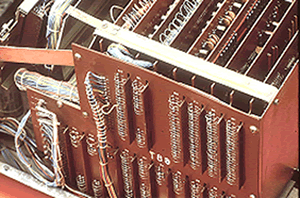
Early devices often utilized masses of discrete hand-soldered wires between subassemblies, a process that added cost and complexity, introduced error, and made repair difficult.
The industry needed a reliable and cost-effective separable interface to provide a mechanism for low-cost assembly, upgrade, and repair. Breaking a system into pluggable modules provided a way to partition the product into subassemblies that enabled the production of electronic products in large quantities. The introduction of the edge connector filled that void.
The concept of the one-piece edge connector is pretty simple. A vertical connector mounted on a motherboard is mated with tin- or gold-plated fingers located on the edge of a daughtercard.

The edge connector enabled the introduction of backplane architecture, in which multiple daughtercards plug into a backplane. A series of copper traces on the surface and embedded within the backplane allows each module to communicate with others in the assembly. The per-line cost of the one-piece edge connector has traditionally been considered one of the lowest in the industry.
 Edge connectors have evolved in multiple directions over the years. Responding to requirements for tighter packaging density, contact centerlines have been reduced in a steady progression from 0.156 inches to 0.8mm and less today. Single-sided PCBs used in consumer products often utilized edge connectors using low-cost tuning-fork contacts. Demand for higher pin counts resulted in double-sided connectors sporting contact designs such as shepherds’ crook, leaf, and bifurcated bellows to address specific application requirements for reliability, high current, or reduced insertion forces. Full gold-plated contacts gave way to highly selective plating technology that placed a gold strip only on the portion of the contact that makes physical contact to the PCB pad.
Early edge connectors featured solder loop tails for termination to discrete wire or long wire-wrap tails that extended through the backplane. Terminating these connectors was a labor-intensive process. Today, most edge connectors are attached to a motherboard or backplane using thru-hole wave/reflow solder or compliant pin technology.
In spite of their low cost, in some industries edge connectors fell into disfavor in the late 1980s due to reliability concerns. Since the edge connector mates with plated pads located on the edge of the daughtercard, the reliability of the interface depends on the ability of the PCB fabricator to assure dimensional and plating control compliant with connector manufacturer specifications. Failure to control factors such as pad plating thickness and porosity, locational tolerance, board warp, PCB thickness, and quality of the leading-edge chamfer can have a major impact on the reliability of the interface. Since the connector manufacturer can control only their half of the interface, a failure can result in blame being tossed between the connector and board vendors, leaving the OEM in the middle without a solution. Under the right conditions, tin-plated contacts and mating PCB pads can develop a nasty habit of fretting, which, over time, could result in an open circuit. Field service people could temporarily solve the problem by simply removing and reinserting the daughtercard, exposing a fresh tin oxide-free surface. Introduction of “gas tight” contacts solved the problem.
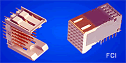 As an alternative to the edge connector, two-piece connectors typically feature a pin and socket interface. Manufacturers of two-piece connectors control the design and manufacturing of both halves of the mating interface, thus improving reliability and taking responsibility for overall quality of the interface. Due to the expected long service life of commercial computing and telecommunications equipment, two-piece backplane connector systems such as 2mm HM and DIN Eurocard became the preferred interfaces. These connectors have continued to evolve as data transfer rates moved into the multigigabits. Recently introduced high-performance differential pair two-piece backplane connectors feature internal shielding structures, tightly controlled impedance, and optimized PCB footprint designs.
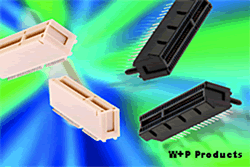 Throughout this period, edge connectors remained a key interconnect. Starting with the ISA and later the PCI peripheral bus, the edge connector continues to serve as the primary internal interface for attaching hardware to the personal computer. The latest iteration of the PCIe specification defines a series of optimized edge card connectors.
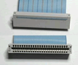 Edge connectors using insulation displacement technology attachment to flat-ribbon cable have been available for many years, and were used extensively to bus storage circuits within a PC.
The use of an edge connector interface is not limited to traditional daughtercard low-speed signal applications. Improved interface modeling and simulation results have proven that optimized edge contacts can perform surprisingly well in multi-gigabit circuits.
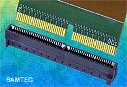 3M and Samtec, among others, have introduced card-edge backplane and mezzanine connectors that are rated to 15 Gb+.
Hirose offers a family of high-speed mezzanine connectors that utilize a PCB interposer card that establishes the spacing between the host and mezzanine card. The same vertical card edge connector is mounted on both boards.
The Micro TCA backplane specification created by PICMG defines a 170 position backplane connector with edge card contacts on a 0.75mm pitch, and is being deployed in low-end 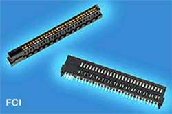 telecommunications applications.
Suppliers including Amphenol, FCI, Molex, and TE Connectivity offer edge card connectors designed specifically for application in power distribution circuits. These connectors mate with large gold-plated PCB pads or with copper bus bars. Individual contact power rating ranges from 9 to over 40 amps per contact. Hybrid versions that contain both power and signal contacts are available.
In recent years, the card edge connector has experienced resurgence in high-speed applications. A combination of superior signal integrity, high signal density, and low cost has resulted in a new wave of connectors that use optimized card edge interconnect technology.
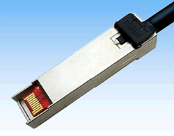 The Molex iPass interconnect system utilizes a card edge interface using flat blanked contacts on 0.8mm centerlines. It has been adopted by a number of standards organizations, including Infiniband, Fiber Channel, and mini-SAS that take advantage of its high-speed characteristics of up to 10 Gb/s. SFP+ and QSFP+ pluggable small-form factor I/O connectors use a highly engineered right-angle edge card connector that mates with gold fingers on a thin PCB.
Currently rated to 10Gb per channel, optimized QSFP+ versions are being pushed to speeds approaching 25Gb/s.
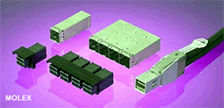
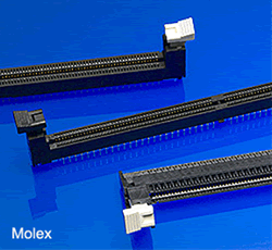
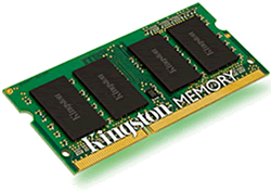 Pluggable memory sockets mating to gold pads on the memory module allow quick installation and upgrading of DDR-3 SDRAM and SO DIMM memory modules. The extremely short electrical path contributes to the high data transfer rates of these edge connectors.
The lowly edge connector, in all of its many configurations, is an example of a legacy interface that has stepped up to the challenge of high-speed and high-density applications. Its original attributes of low profile and cost have been applied to current and next-generation products that will continue to extend the life of this unique interface or many years.
No part of this article may be used without the permission of Bishop & Associates Inc.
- Optics Outpace Copper at OFC 2024 - April 16, 2024
- Digital Lighting Enhances your Theatrical Experience - March 5, 2024
- DesignCon 2024 in Review - February 13, 2024


