Meeting Datacom and Telecom Application Demands With Higher Data Rates and Smaller Connectors
As the need for bandwidth continues to increase, so does the need for higher data rates and smaller connectors capable of higher densities. What was once 1–3Gb/s moved to 4–8 Gb/s; then we saw the jump to 16Gb/s, then 28Gb/s, and now we are ready for 56Gb/s.
Although the datacom and telecom industries are pushing for higher data rates and smaller connectors capable of higher-density configurations, achieving this performance is much easier said than done. Design challenges include routing complexities on the PCB and the potential need for higher layer counts. Additionally, for longer trace lengths, more exotic PCB materials with lower dielectric constants and retimers are incorporated to mitigate degrading signal loss. All of these factors add more cost to the system.
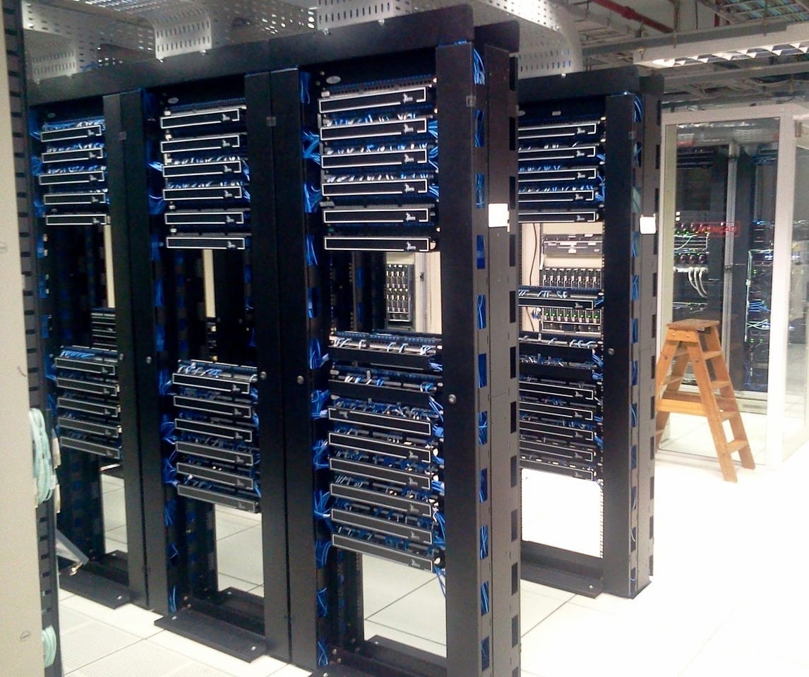
Data centers are one of many applications fueling higher bandwidth demands.
Besides materials and costs, designers also frequently face challenges with the decreasing size of the finished products. The proliferation of mobile and handheld devices drives this trend, as well as new requirements in industries such as telecom, high-power computing, medical devices, aerospace and defense, and even industrial.
In addition, new high-data-rate chipsets, which are especially designed to generate as little heat as possible, still produce heat. In fact, these often require more and bigger heat sinks, further complicating the design dilemma.
Obviously, the increasing demand for smaller, higher-bandwidth PCBs pushes R&D in the interconnect industry. Sales of both micro-pitch and high-speed interconnect systems steadily increase. The interesting caveat is that most high-speed interconnects are also micro-pitch. However, the smaller the interconnect pitch, the more difficult it is to achieve higher bandwidths.
Smaller and tighter-pitch interconnect systems introduce a new set of electrical challenges, including crosstalk and insertion loss. This is primarily due to the proximity of one differential pair to the next, reduced space for routing, and a reduction in grounds pins.
As with many design challenges, there are several ways to address the problem.
PCB Layout
Designers can alleviate some of these conditions by being strategic about their board layout. Well-planned trace design and routings and the location of grounds, vias, and other components improve PCB data rates. PCB design strategies are beyond the scope of this article, but numerous tools, resources, and personnel exist to assist in this endeavor. Samtec, for example, has the Signal Integrity Group and Teraspeed Consulting to assist in these matters.
High-Speed, Micro–Pitch Interconnect Design
Although the goals of miniaturization and higher data rates often conflict, connectors can strike a balance between performance and footprint size.
One example of these connector design strategies is a contact called Edge Rate®. This contact is designed to deliver high cycle-life and support high-bandwidth. For example, the 0.8mm-pitch Edge Rate interconnect is rated at 56Gb/s PAM4. One of the ways it achieves this balance between bandwidth and pitch is the design and placement of the pins within the plastic body. The thin, narrow, cut edges of the Edge Rage contact are positioned side-by-side, which minimizes the parallel surface areas and effectively reduces broadside coupling and crosstalk.
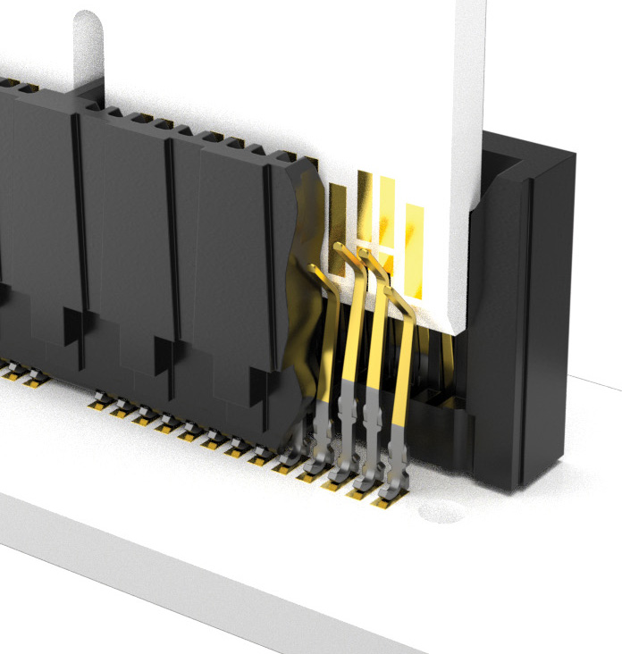
A high-speed, micro-pitch Edge Rate socket from Samtec.
Improving Connector Performance
Other connector design strategies to achieve high-bandwidth, micro-pitch interconnects include, but are not limited to:
- Performing multiple simulation cycles in the early stages of the design in order to accurately quantify product performance before you begin the expensive tooling process.
- Minimizing the stub in the contact area when the connector is mated. Mechanically, the longer the stub the better for reliability, but longer stubs are an electrical liability, as they act like an antenna.
- Simplifying contact geometry for improved signal path performance.
- Shortening the pin length to minimize the distance the signal must travel.
- Incorporating asymmetrical footprints and contacts wherever possible. Alternating designs decrease crosstalk from pair-to-pair both within the row of pins and between rows. In other words, the footprint should drive the connector performance.
- Optimizing the connector break-out region (BOR). Think of the connector as a critical node in the link. Don’t limit your focus to the node; consider the link as well.
- Incorporating common ground planes into the connector, space permitting.
- Choosing plastic molding beneficial to connector performance. Among other concerns, carefully consider: high-temperature plastic for RoHS, matching dielectric constant (Dk) for the desired impedance control, and dimensional stability over temperature and time.
The bottom line is, the shorter and straighter the signal path and connector contact, the better the signal integrity performance. However, to achieve the right balance, the connector must have adequate normal force and withdrawal force, as well as a certain degree of ruggedness, and these considerations usually detract from the signal integrity performance.
Flyover™ Technology
System architects are now using an alternate approach that reduces the use of PCB traces to conduct high-speed signals. Instead of increasing layer counts, which involves using costly high-performance PCB materials and dealing with long, degrading trace lengths, the signals are taken out of the board using a cable. Samtec refers to this technique as Flyover™. Flyover improves signal integrity performance, allows for higher signal speeds, and reduces the overall cost of the system.
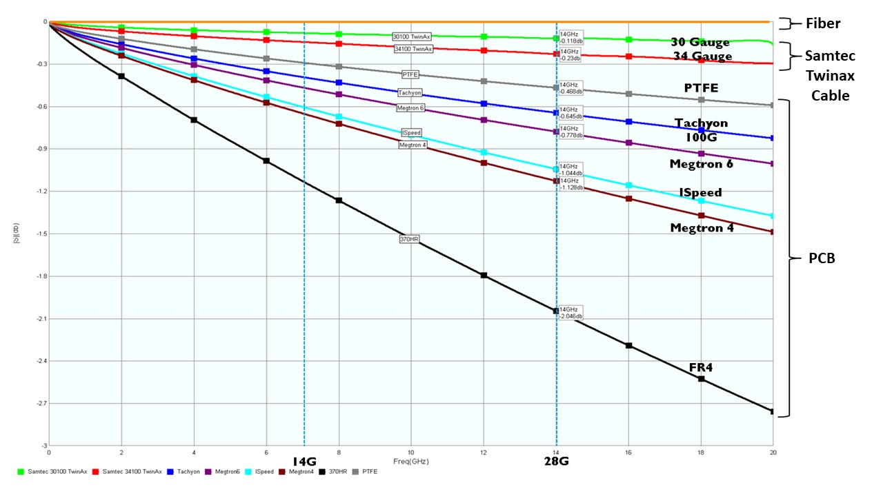
Comparison of bandwidths that can be achieved using various materials.
In typical applications, a connector is positioned as close to the chipset as possible, and then a discrete or ribbonized twinax cable is used to either pass the signals to another location on the board or attach directly to an I/O connector. Depending on the system layout, there are multiple connector options to work around the available space, such as a low-profile horizontal connector that would attach underneath the chipset heat sink.
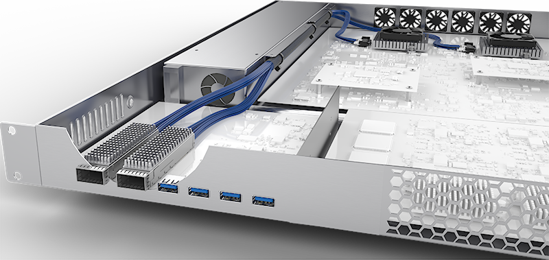
A Samtec Flyover™ application.
Flyover technology offers many advantages. First, it can achieve high data rates of 28, 56, and 112Gb/s and beyond with minimal loss. Since it removes the high-speed signal from the PCB it allows users to reduce the layer count, remove any retimers that were in place, and utilize a more common PCB material, all of which helps reduce the overall cost of the system.
However, producing a high-speed cable assembly system to achieve these performance goals is difficult. Among the many pieces in the puzzle are the mating connectors, the transition boards in the cable assemblies, the PCB routing strategies, and, of course, the cable itself.
Samtec incorporates its ultra-low-skew twinax cable technology in high-speed cable assemblies. Co-extruded twinax cable technology eliminates the performance limitations and inconsistencies of individually extruded dielectric twinax cabling. This improves signal integrity, bandwidth, and reach for high-performance system architectures.
Although the goals of miniaturization and higher data rates conflict, connector manufacturers can strike a balance in data rate performance and footprint size. Interconnect contacts can be designed to minimize size and maximize bandwidth. The plastic materials in the connector insulator also affect performance, and alternative strategies, like taking signals off-board with high-speed cable systems, can effectively address the challenges of speed and cost.
By Kris Erickson, Director of Business Development, and Danny Boesing, Product Marketing Director, Samtec, Inc.