Co-Packaged Optics Are On the Horizon
A progression of system packaging options provide a roadmap to supporting the high speeds inherent in next-generation equipment. As 112G becomes a reality, co-packaged optics offer the best signal integrity.
Since the advent of multigigabit signaling, design engineers have struggled to find ways to minimize the negative effects of conducting high-speed signals through copper traces embedded in PCB laminate material. Co-Packaged Optics

Ensuring signal integrity (SI) requires the design of circuits capable of delivering a recognizable signal over a defined distance with an acceptable bit error rate (BER). A host of factors, including attenuation, forward/backward crosstalk, skew, jitter, reflections, switching noise, intersymbol interference, and return loss nibble away at the quality of the signal. The degree of impact these factors have on signal integrity increases with signal speed and the length of the channel.
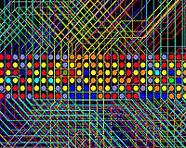 To address these challenges, engineers adopted multiple strategies. The layer count was increased with layers dedicated to signal isolation. Plated through holes became smaller and were back-drilled to minimize stubs. Standard epoxy board materials were replaced with higher performance laminates. Upgraded versions of traditional FR-4 PCB laminate material offer lower loss via reduced dielectric constant (Dk) and dissipation factor (Df), along with improved mechanical and thermal properties. The surface roughness of the copper as well as moisture absorption of the laminates were recognized as sources of signal loss. Even tiny inconsistencies in the glass weave of the PCB substrate can degrade a high-speed signal. More exotic laminate materials, such as MEGTRON6 and the new MEGTRON7, have become the gold standard for high-end performance, but they come at a significant increase in cost.
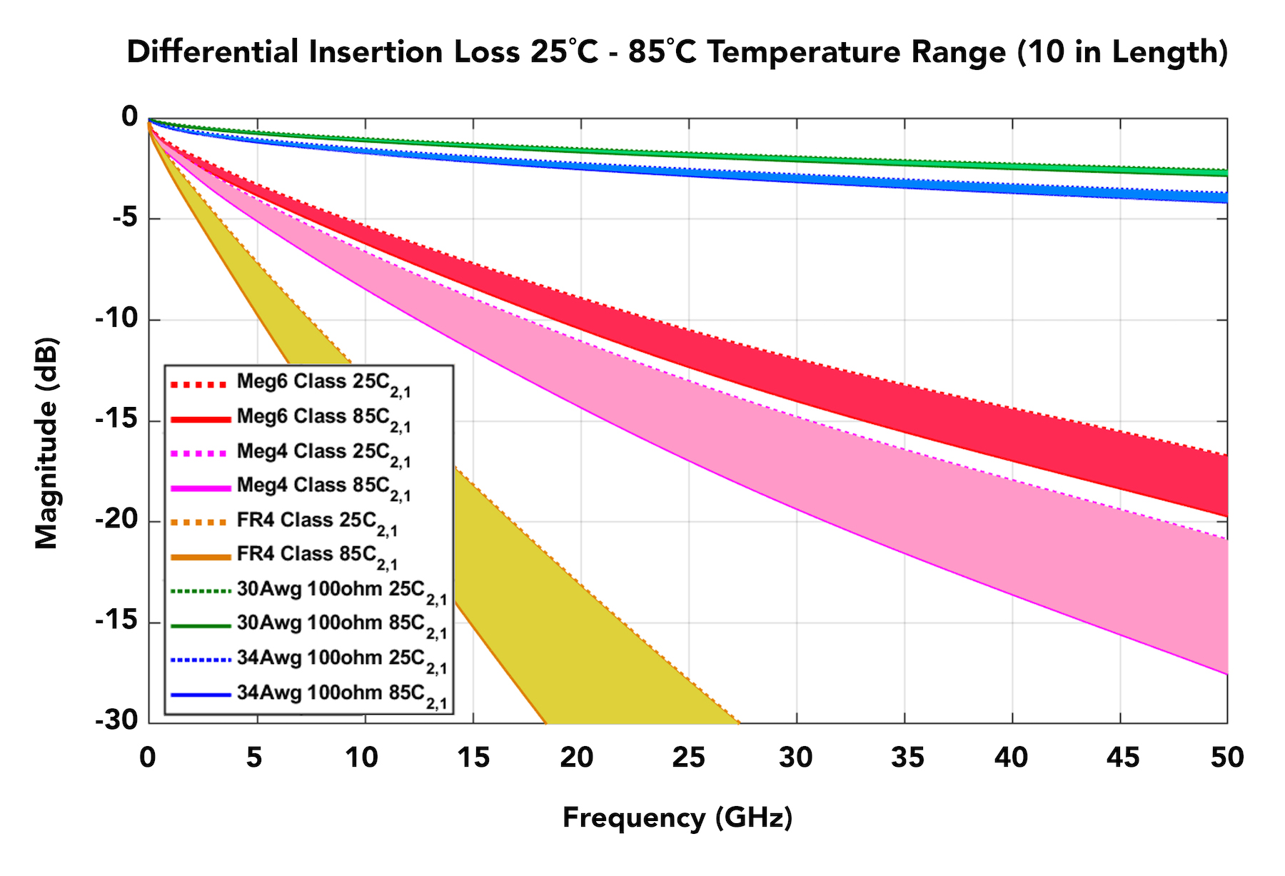
As data rate requirements approach and surpass 112Gb/s PAM4, developers are challenged with balancing increasing throughput, scalability, and density demands with concerns such as power consumption, signal integrity, time-to-market, and cost. To hit these speeds, designers often have to use special board laminate materials with lower dielectric constants and dissipation factors. However, these materials are expensive and even with these exotic materials, the trace lengths on the boards are still relatively short. As the chart above shows, even when using expensive, high-speed PCB materials, it’s difficult to have trace lengths of any significant distance, as shown in this analysis by Samtec.
As bandwidth increases, levels of loss and distortion may become unacceptable. Designers began to bump up against the maximum practical length of a high-speed channel as dictated by the characteristics of even the best PCB laminates and board design practices.
One recent solution has been to take the highest speed signals out of the board and “fly” them over the PCB surface via shielded twinaxial cable. The loss and noise characteristics of shielded twinaxial cables is much lower than through PCB traces. Signals are launched as close as possible to the source, such as an ASIC, SERDES, or processor chip. These cables can be terminated to another location on the same PCB or directly to the input/output panel.
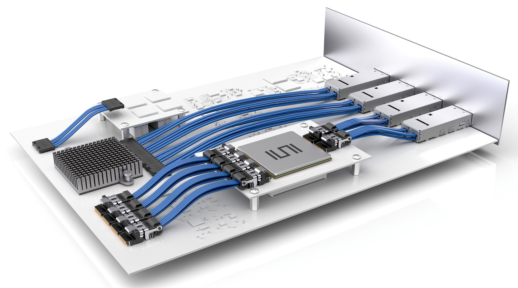
Samtec’s FireFly™ Micro Flyover System™ has expanded to enable a variety of board-to-board and board-to-I/O interconnects, including a board-directly-to-a-QSFP-connector.
The current technology roadmap includes channels operating at 56Gb/s to 112+Gb/s. At these rates, designers face serious performance and reach limitations.
Rather than utilizing copper traces embedded in a PCB or twinaxial cable, a designer can choose to conduct high-speed signals via optical fibers. A mid-board optical transmitter converts high-speed signals to optical pulses, which can be directed to another location on the board or to the I/O panel. Locating an optical transceiver near an ASIC or switch reduces the lossy PCB trace length to a minimum while increasing channel reach. Optical fiber can be terminated with a variety of miniature optic connectors, significantly improving I/O panel density.
Multiple organizations have defined a progression of system packaging options that provide a roadmap to supporting next-generation equipment. Starting with current PCB traces extending from a switch to the I/O, a mid-board optical engine significantly reduces copper losses. The next step locates the optical engine on the same substrate as the switch. The ultimate solution may be the integration of optics directly into the switch chip.
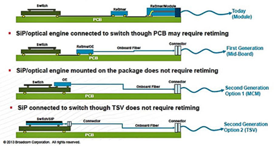
The evolution of optical I/O line card implementations for increased bandwidth is shown in this Broadcom illustration of four generations of packing options.
The Consortium for On-Board Optics (COBO) is a collaborative organization that was formed to develop specifications facilitating the use of board-mounted, interoperable, and interchangeable optical modules. COBO is focusing its standards development efforts on the manufacturers of networking equipment, such as switches and servers. COBO module attachment is based on a two-piece surface mount connector system. Modules simply cam and lock down.
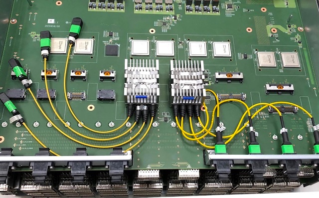
Delta collaborated with COBO to develop a proof-of-concept open networking switch featuring 12.8Tb/s bandwidth capacity as well as the seamless integration of five different optical module form factors in a single 4U rack.
Co-packaged optics, or chiplet optics, is a rising technology that addresses some of the challenges created by small form factor pluggable optical transceivers, including thermal management, power consumption, bandwidth, and port density. The objective is to move the electro-optic conversion process as close as possible to the compute, switch, or ASIC die to achieve higher bandwidth and energy efficiency. The active device and optical transceivers are mounted on the same substrate, eliminating all loss and distortion attributed to copper traces on the motherboard.
Electrical signals from the chip are converted to optical signals by the photo integrated circuits (PICs), also known as opto-chiplets, located on the periphery of the substrate and coupled to optical fiber. These fibers are terminated to high-density optical connectors, which can be mounted on the I/O faceplate.
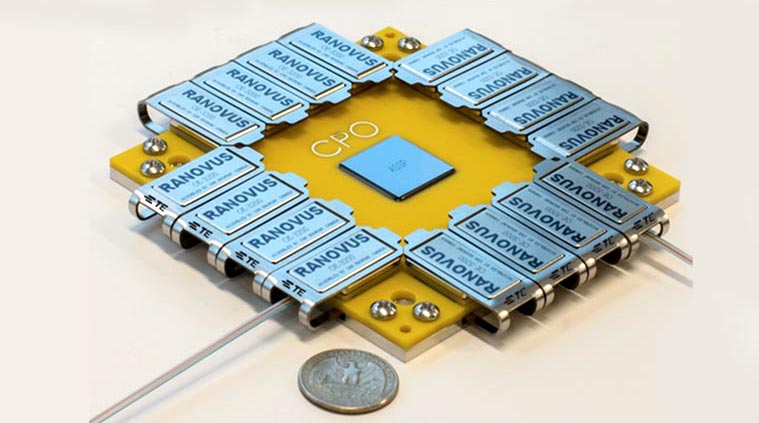
Ranovus collaborated with TE Connectivity, IBM, and Senko Advanced Components to design multi-vendor, co-packaged optics solutions. TE Connectivity demonstrated this technology at DesignCon 2020.
Small profile passive optical connectors, such as MPO or MXC, mounted on the exterior of a 1RU faceplate can dramatically increase port density and channel count.
The advantages of locating optical transceivers on the same substrate as a high-performance chip include:
- Reduced power consumption, as the SERDES or switch chip does not require high-power I/O drivers. Improvements of up to 20% are possible.
- Greater system reliability, as signals are spread among many separate laser sources. Failure of a single laser will not take down the system.
- Increased bandwidth scalability.
- Improves I/O port and overall system density. Optical pluggables may have reached their density limits.
- Reduced chip-to-I/O loss/distortion.
- Minimizes requirements for retimers.
Some design concepts call for a pluggable interface at both the substrate and front I/O panel or backplane, while others feature a permanently attached fiber optic pigtail at the optical engine.
In March 2020, Ranovus announced a strategic collaboration with IBM, TE Connectivity, and SENKO Advanced Components to create a standard platform to design and manufacture multi-vendor solutions for co-packaged optics. They launched the Odin single-chip silicon photonic engine for data center applications. At 100Gb/s per lambda, the Odin optical engine can scale from 800Gb/s to 3.2Tb/s with a single chip. Additional major chip suppliers, including Intel, IBM, and Rockley Photonics have announced co-packaged optical modules.
Co-packaged optical devices face some daunting challenges, especially in the establishment of standards, but large cloud providers, including Facebook and Microsoft, are determined to create guidelines for equipment designers and manufacturers of co-packaged optical modules.
The Optical Internetworking Forum (OIF) has been particularly aggressive in the development of standards that support next-generation, high-speed optical packaging architectures. They recently sponsored a webinar outlining some of the issues involved in creating a specification for co-packaged optics. In November 2020, OIF announced the launch of the Co-Packaging Framework Implementation Agreement Project, which will identify co-packaged applications and their requirements, as well as initiate standardization activities.
The development of co-packaged optics is an important technology to watch, as it offers improved high-speed performance with the potential to threaten the current crop of small form factor pluggable options, including the most recent QSFP-DD and OSFP. Designers of equipment destined for mega data centers and cloud applications see co-packaged optics as a potential solution to increasing demands of speed, capacity, and reduced power consumption. It is unclear at this time if co-packaged optics technology is a long-term solution or simply an interim step towards optics being directly integrated into high performance chips.
Like this article? Check out our other Fiber Optics, High-Speed, and New Technology articles, our Datacom/Telecom Market Page, and our 2020 and 2019 Article Archives.
- OFC 2026: High-Speed Networking in the AI Era - April 7, 2026
- DesignCon 2026 - March 17, 2026
- Breaking Through the AI Power Wall - January 20, 2026


