Porosity – The (w)Hole Story
Porosity – The (w)Hole Story is all about the defects
Sorry about the title, but I couldn’t resist.
Porosity consists of small (microscopic) defects in a plated coating. In connectors, a typical plated coating thickness for noble metals (gold and palladium alloys) is in the range of 0.1 to 1.25 microns (4 to 50 microinches). As Max Peel noted in his article in the last issue, porosity depends on plating thickness and is not generally a problem at thicknesses greater than 1.25 microns. Let’s consider this thickness dependence from a physical point of view.
The following description is somewhat simplistic but illustrates the essential concerns at issue: The plating deposits on the substrate appear in a discontinuous manner, nucleating at numerous sites on the substrate. The plating spreads out over the surface as it increases in thickness and the growing islands of plating eventually coalesce to completely cover the surface. Early in this coalescence process, the issue is surface coverage and towards the end, it becomes porosity. In connector-speak, thin gold, or flash, platings, of the order of 0.1 microns, are in the surface coverage regime. This is a different issue than porosity in that it is intrinsic to the plating process. Surface coverage will always be an issue in flash gold platings. Porosity, in contrast, is process-dependent.
A typical noble metal plating includes a nickel underplate over the contact spring base metal, usually a copper alloy. The nickel underplate provides many performance benefits, as described in previous articles. One of the benefits is that nickel plating (typically 1.25 to 2.5 microns) can bring the porosity down to low levels; it, too, is process-dependent. In the ideal case this means that when the gold plating is applied, any gold porosity will generally be to the nickel surface. As described in Max’s article, the nickel provides a passive protective surface in contrast to the corrosion that would take place if the pore extended down to the copper alloy base metal. This pore passivation is a second benefit of nickel underplates.
Let me call your attention to the italicized “ideal case” in the previous paragraph, because the real world of connector plating is not ideal. There are three major sources of non-ideality: The base metal substrates are not perfect, the stamping and forming processes used to create the contact geometries are not perfect, and the plating processes themselves are variable. Let me immediately state that all of these processes can be performed with high levels of quality and consistency, but “ideal” is an exceptional goal. Strip metal manufacturing processes produce strip surfaces with controlled roughness, but occasional defects are possible. The same potential for defects exists in the stamping, forming, and plating processes. The low porosity levels that can be realized are testimony to the quality of these processes as they are practiced today.
But the presence of such defects can be a source of porosity. The plating must “bridge” over any defect to produce a pore-free surface. Such bridging may require significantly more thickness than the ideal case, with porosity being the result in the range of plating thicknesses used in connectors. The magnitude of “significant,” of course, depends on the nature and severity of the defect.
What is the performance concern of porosity? Max’s article addressed some of the issues — corrosion and corrosion creep. Figure 1 provides additional insight on corrosion creep.
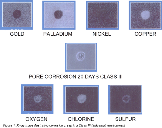
Figure 1 contains X-ray maps of a pore corrosion site. The sample shown was a gold-flashed palladium over nickel over phosphor bronze contact. An X-ray map is obtained from a Scanning Electron Microscope (SEM). The SEM shoots an electron beam onto the sample surface exciting all the atoms beneath the beam. Each excited atom, in turn, releases a characteristic X-ray of a particular energy. A detector is set to detect only the specific characteristic energy, say of gold.
The gold X-ray map is white, from impinging characteristic X-rays, where gold is present. The dark areas indicate a pore site. The pore site is clear in the gold and palladium by the absence of signal, and in the copper, exposed at the base of the pore, by the presence of signal. The nickel map is ambiguous because the nickel X-rays are absorbed as they pass through the palladium and gold layers. The presence of copper indicates that the pore site in this sample went all the way through the gold, palladium, and nickel to the underlying base metal. As noted, copper alloys are susceptible to corrosion so the exposed copper at the base of the pore is a corrosion source. The middle SEM photograph shows a corrosion product ring around the pore site. The lower three maps were obtained by setting the detectors to the corrosive species, in this case, oxygen, chlorine, and sulfur. Note that the oxygen and chlorine stay in the vicinity of the pore site while the sulfur migrates away from the pore site. This tells us that the corrosion products in the rings are primarily a combination of copper/sulfur. The concern with porosity is the potential for corrosion and corrosion creep at and around the contact interface that results in increased contact interface resistance. The potential for increased contact interface resistance is enhanced if the contact interface is susceptible to fretting motions due to inadequate contact mechanical stability. (Yes, that brings up one of my favorite topics, contact normal force, but I’m not going there this time.)
The potential for corrosion creep depends on the application environment, in particular the presence of chlorine and sulfur. This dependence is evident in the flowing mixed gas test environments for noble metal platings, which include ppb levels of H2S, Cl, NO2, and, in some cases SO2. The rates of corrosion creep are material-dependent. Generally corrosion creep rates are highest for gold surfaces, lower for palladium and palladium alloys, and lowest for nickel surfaces.
To complete the (w)Hole story we must revisit flash platings. As noted, flash platings are a surface coverage issue. It is important to note that the X-ray plating thickness measurement technology does not provide a thickness measurement directly. Rather, it measures the mass of the plated material and the thickness is calculated from the (assumed) plating density and the area of measurement, or it is based on comparison to established thickness standards. For flash gold, the plating density is indeterminate due to incomplete surface coverage, and a meaningful standard is questionable. The important point is that a gold flash X-ray thickness measurement will only be a guesstimate, with the actual point-to-point thickness varying significantly above and below that guesstimate. In addition to the surface coverage issue, the mating “durability” of a flash gold is, to say the least, limited. In sum, the contact interface of a flash gold plating will in all likelihood be or become the plating beneath the flash.
- Nanocrystalline Silver Alloy Contact Finishes in Electronic Applications - April 6, 2015
- Nanocrystalline Silver Contact Platings - March 16, 2015
- Dr. Bob on Gold Flash Contact Finishes (and Max Peel) - September 22, 2014