Key Considerations for High-Speed Connectors
A how-to guide for selecting and successfully implementing high-speed connectors
Michael Rock, Engineering Manager – Signal Integrity Products, AirBorn Inc.
When designing applications that utilize high-speed interconnects, it’s vital to navigate around all potential speed bumps along the signal’s path. Factors including: stackups, tolerances, via design, trace widths, plating, and copper etching must be understood and mastered to achieve optimal signal paths. Any design checklist should also include the connector, which oftentimes is overlooked. If not scrutinized, connectors could wreak havoc on a system’s signal integrity.
A proper connector should provide a few key elements:
- Matched impedance over the bandwidth of interest
- Low insertion loss over the bandwidth of interest
- Reliable connectivity to the PCB
- Reliable connectivity to the cable system
In order to ensure that the connector provides low loss and matched impedance to the signal, one must look at scattering or s-parameters. S-parameters specify the nature of linear electrical networks and identify the bandwidth and the loss of a circuit, providing a peek into its performance potential. S-parameter data is provided by manufacturers as a way of characterizing their connectors, and should be the first criteria considered when high-speed connectors. Designers should also transform and observe s-parameters in the time domain, as a time domain reflectometry (TDR) plot and see what the impedance profile looks like internally.
Since connectors are available in a good many flavors (e.g., termination styles, internal signal lengths, materials, etc.), designers need to understand how the s-parameter files were created. It’s important to ask the vendor several questions before blindly placing a touchstone file into a simulation and trusting the results, including:
- Does your intended pinout match the simulated one?
- How were the other pins terminated?
- What layout was used in the provided data?
- Are there any stubs?
- What was the termination style used for characterization? (e.g., plated thru-hole, surface-mount, press-fit)
- How was the fixture de-embedded or what’s included in the measurement?
- Is this the exact part number I need?
Quality suppliers provide simulated and measurement-correlated data for each customer’s intended use to provide them with a more accurate assessment of the connector’s impact on the design and bolster their confidence levels in the simulated data.
Another important criterion when selecting connectors is PCB termination options. Connectors typically come in several termination styles, including (but not limited to) surface mount, press-fit, and paste-in-hole (PIH), each of which has distinct strengths and weaknesses. Press-fit terminations are very rugged and provide maximum retention and connectivity to the PCB, but also present a tough challenge for high-speed applications. Routing a signal out of a high-density press-fit connector may require a high layer-count PCB, presenting the longest path up through the plated holes to get to the connector. The elongated route and fixed diameter of the drill holes can produce significant discontinuity for higher frequency signals and may hinder high data rates.
A surface-mount termination is more amenable to high-speed design and allows for maximum flexibility when matching impedances at the connector launch point. Designers can route directly into the pad of a connector or use a drill hole of choice to provide a path up through the PCB. In addition, the vias can be buried within the PCB or back-drilled to reduce the unused via stub and improve the frequency response over the press-fit termination style. This termination method offers the most benefits for high-frequency design, but is not necessarily robust. Surface-mount connectors normally require some additional reinforcement, such as mounting hardware, to ensure a strong connection to the PCB.
PIH terminations are somewhat of a hybrid between the previous two styles. Similar to press-fit, PIH terminations have a shorter, non-press-fit pin that is inserted into a plated through-hole footprint and soldered in place. The main difference being that the pin is much shorter and the holes can be back-drilled to remove the excess stub on the signal. High-density connectors of this sort can still be a challenge to break out into the PCB. Select suppliers offer these pins as short as 10mm to provide improved high-frequency response and a rugged connection to the PCB. Each termination style has some discontinuity in signal impedance as it transitions from the PCB to the connector, and each allows the designer varying degrees of freedom to minimize the discontinuity’s impact on signal integrity.
When selecting connectors for high-speed designs, it’s also important to consider how it contacts the mating connector. There are several methods of mating contact, each with its own unique set of benefits and limitations that affect the signal integrity of the overall design. Edge-mount connectors are one popular mating contact method. These connectors have spring-loaded fingers that slide along the PCB pad to make electrical contact at a single point, which allows for minimal discontinuity in the signal, but may prove detrimental (or require additional retention methods) in high shock and vibration applications. Many MSA-standard designs (e.g., SFP, SFP+, and QSFP) use this type of electrical interface.
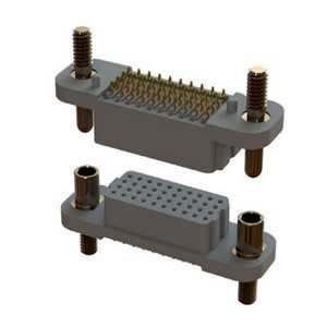
Press-fit connections are more widely-used in rugged applications. This fairly basic system is comprised of a female side with a socket and a male with a spring pin designed for socket insertion. This mating category has two or more points of contact and can offer several advantages over the single point of contact offered in edge-mount mating systems. Especially designed for high-reliability, high-speed products, the multiple contact points pictured in Figure 1 present a lower contact resistance and inductance to the signal, as well as a reliable and rugged connection sure to withstand extreme vibrations. However, pin and socket contacts can be longer than edge contacts, which could present a larger discontinuity if not designed properly. So, it’s crucial to study the s-parameters and impedance plots provided by the manufacturer.
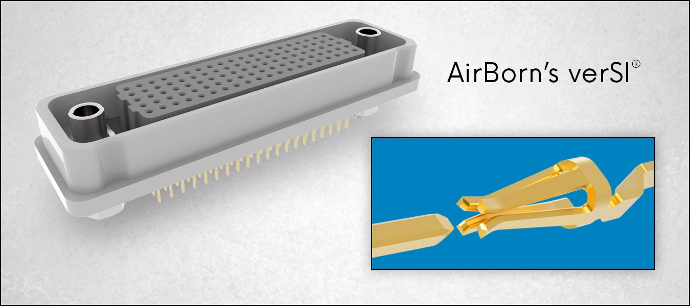 Figure 1: Airborn’s verSI® press-fit pin and socket connectors deliver robust, reliable, low-inductance connections in high-speed applications subject to extreme vibrations.
Additionally, when designing for speed, it’s important to consider the throughput relative to the footprint. Figure 2 compares two basic systems: one with 25G/lane QSFP connectors and one with 10G/lane HD4 connectors. The resulting output (4320Gbps vs. 3600Gbps) shows that superior density achieved through connector design can result in greater data throughput with 10G HD4 connectors than higher-speed 25G QSFP connectors within the same rack system, providing savings on components and energy costs, and potentially even data center square footage.
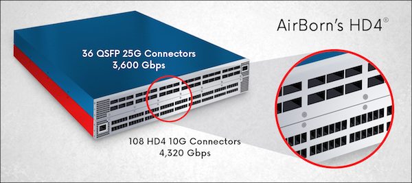 Figure 2: Designed for superior density, AirBorn’s 10G HD4® connectors can provide greater throughput than 25G QSFP connectors within the same rack system, enabling component and energy cost savings.
At the end of the day, designers need to get a strong, undisturbed signal from Point A to Point B, and a proper connector is a critical element along that journey. After all, even the highest-speed connectors aren’t beneficial if they experience intermittent opens. The highest quality suppliers offer a wide selection of connectors for high-speed and high-reliability solutions, end-to-end channel solutions, work closely with customers to assess their individual needs and develop optimal interconnect solutions with minimal signal degradation. Designer have numerous connector options to choose from and should thus pay close attention to the associative data and choose wisely.