Chip-on-Tip Technology Enables Minimally Invasive Medical Devices
Chip-on-tip endoscopy technology relies on microminiature sensors, illumination, and lenses. Market pressures are driving these critical medical devices to shrink in diameter and cost while maintaining, if not adding, functionality. Meeting these demands requires ingenuitive engineering and manufacturing techniques.
Chip-on-tip technology is dramatically improving medical care by enabling minimally invasive imaging. The term chip-on-tip typically refers to the placement of an imaging sensor on the distal tip of a device such as an endoscope, which can be inserted into the body to provide healthcare providers with images of internal organs. Advancements in sensor, LED, lens, molding, data transmission, and sealing technologies, and especially significant size and cost reductions, are allowing chip-on-tip technologies to expand into new regions and product areas.
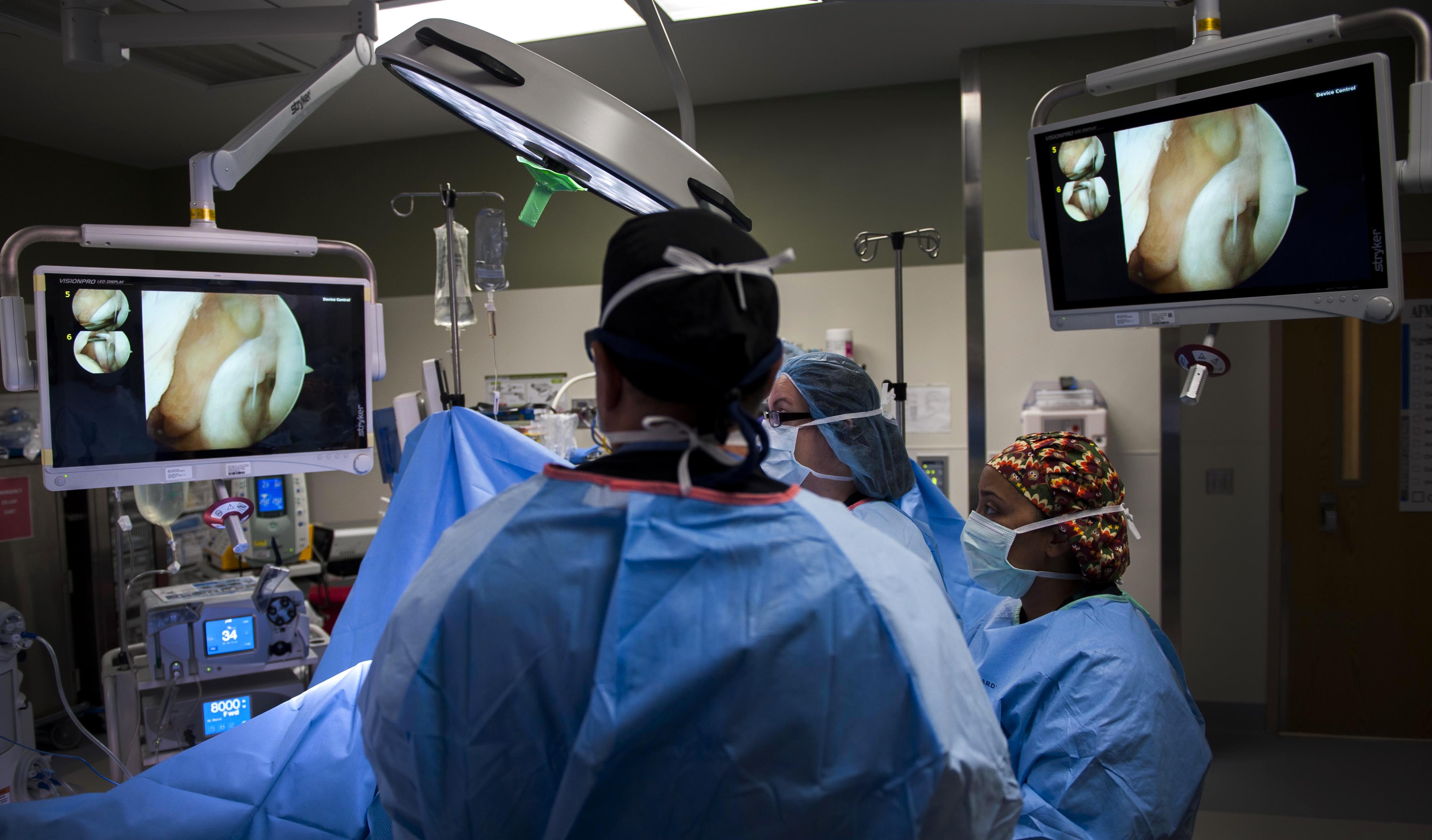
An orthopedic surgeon uses an endoscope to repair a soldier’s torn ACL.
Image Sensors and Chip-on-Tip Technology
Image sensors convert received light into electrical signals and are typically based on charge-coupled device (CCD) or complementary metal-oxide semiconductor (CMOS) technologies. CCD sensors were the first deployed in digital photography and endoscope imaging. CMOS sensors became more popular as manufacturing methods improved to permit the fabrication of devices that could rival CCD image quality. The lower power consumption of CMOS sensors also made them attractive to the cellphone industry, which drove further size reductions. It is now feasible to accommodate a CMOS-sensor-enabled camera on the distal end of an endoscope.
Light Emitting Diodes
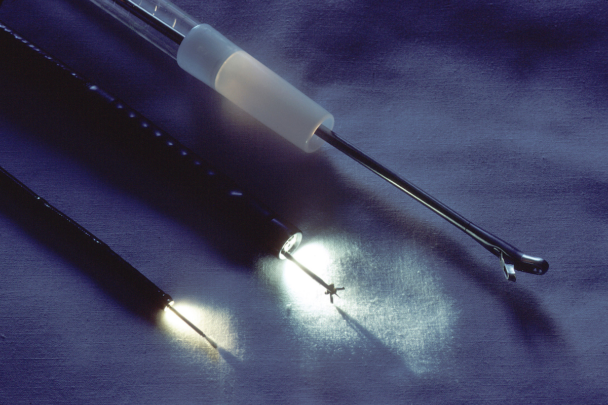
Light emitting diodes ( LEDs) are another enabling advancement for chip-on-tip technology. Over the years, LEDs have evolved to provide bright white light, making them viable for general illumination applications. Miniature LED illumination sources can now be placed on endoscope tips along with CMOS camera, which obviates the fiber optics traditionally used to transmit the illumination from the capital equipment to the tip of the scope. These tiny surface mount technology (SMT) LEDs are currently commercially available in the 0201 package size (0.02” x 0.01”).
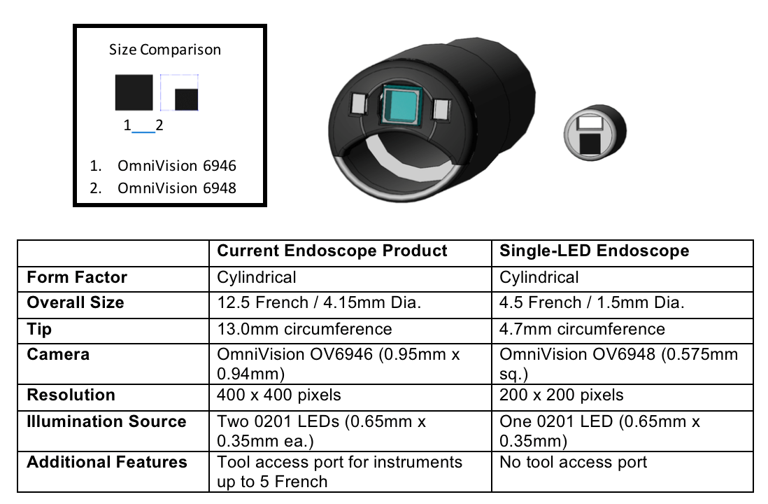
Reduced catheter sizes made possible by CMOS cameras and miniature, 0201 SMT LEDs.
Miniature Lenses
Lenses are another critical aspect of chip-on-tip endoscope systems. There are multiple lens technologies, including systems based upon ground glass elements, plastic elements, and graduated index (GRIN) lenses. The lens system requires careful design to achieve the properties needed for the application, such as viewing angle, focal length, and other factors. The lens systems for chip-on-tip endoscopes typically involve more than one element and thus require some precision in dimensional configuration. Lens stacks can require adjustments made during the assembly into the endoscope tip and along the entire path from the objective lens to the image sensor, but must be sealed to keep fluids out of the optical path.
Overcoming Engineering Challenges for Further Miniaturization
To design and construct a practical chip-on-tip device, the camera and the LEDs need to be mechanically mounted within a tip. In the case of a medical endoscope, it is typically necessary to keep the girth of the tip as small as possible. This means the tip will have very small features and thin walls.
Endoscopy equipment. Image courtesy of the National Cancer Institute.
In the case of single‑use endoscopes, this part is typically made of injection molded plastic, which allows users to create complex shapes in a low-cost manner. However, injection molding parts this small requires specialized micro molding techniques and practices.
Micro Molding Techniques
Micro molding is a specialized segment of the plastic injection molding industry, dedicated to molding parts that are extremely small and/or extremely detailed. Successful micro molding begins with the component part design, through to tool design, and finally to proper molding equipment and processing parameters.
The attributes of conventional molding processes and equipment have limitations that can preclude effective molding of micro-scale parts. Large barrel sizes create problems with material residence times. Managing small shot sizes with the precision needed is not possible for very small shot sizes using large equipment and will result in short shots or flash from overpacking.
Part design can dictate mold construction. With finely detailed micro-scale parts, the tooling to produce them also ends up having micro‑scale features. If the part designer does not consider both mold construction and tooling robustness in the design of the part, the end‑product will be a part that it is difficult or impossible to effectively tool. Without care and robust design review practices, it is possible to create part details that would function perfectly in the finished part but will result in poor mold robustness or complexity of construction. This can result in making the part more difficult or even impossible to produce.
Data Transmission and Integrity
Another challenge is successfully delivering the video image from the chip-on-tip sensor to the display/data capture device. Image sensors have various analog and digital formats for data output, and some are more sensitive than others. The data moving from the image sensor to its destination is susceptible to corruption or distortion from both internal (e.g., power supply) and external (i.e., surrounding environment) electrical noise sources. Preserving signal integrity begins with the design of the circuit to drive the LEDs.
Pulse width modulation (PWM) is a practical way to drive LEDs for several reasons. By employing PWM, the pulse magnitude and duration may be varied to employ a variable intensity (i.e., dimming) function. PWM can also drive the LEDs with a peak current higher than the maximum continuous current to achieve a higher lumen output.
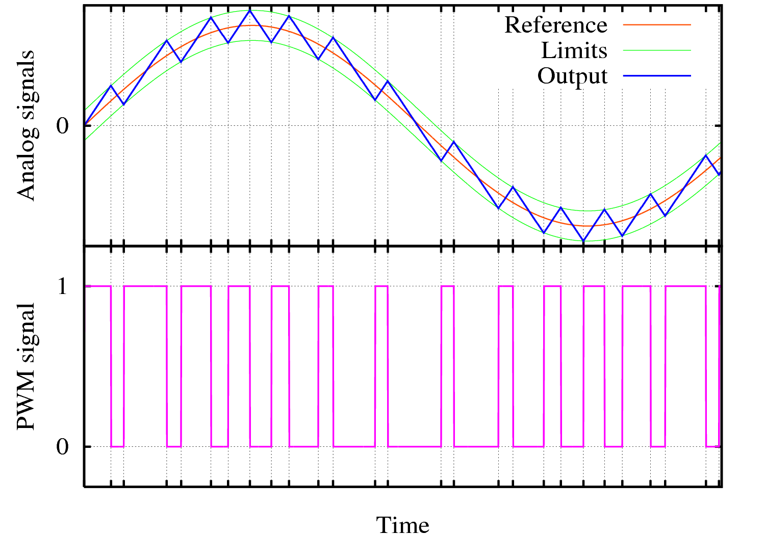
Analog signals vs. PWM signals. Image Credit: Cyril BUTTAY (CC BY-SA 3.0)
However, PWM circuits generate significant electrical noise, whereas pure DC circuits do not. This doesn’t preclude driving LEDs in chip-on-tip technologies with PWM, but the potential effects must be mitigated through the knowledgeable application of shielding techniques and conductor design. Achieving proper shielding in extremely small chip-on-tip designs can be accomplished with micro-coax wiring and flex circuits that employ shielding layers to emulate a coax shield.
The challenge of preserving signal integrity is exacerbated when the distance from the sensor to the display or storage device is increased, reducing signal strength and multiplying opportunities for interference. Solutions in these instances include amplifier circuits and low-loss conductors.
Conductor resistance can be reduced using silver plated wire for up to a 4% gain. Use of low-loss conductors becomes a compromise of increasing conductor size to the limits of the available space. Solutions can be created with alternate geometries to take advantage of the space available. Two examples include employing flat wire and printing conductors directly onto enclosures and cannulae.
Environmental Protection
Of course, the interconnection needs to be environmentally sealed to prevent shorting and other influences of exposure to fluids. In medical applications, this typically means saline solution, bodily fluids, and other substances. Successful sealing begins at the design stage by providing appropriate features for the sealing system to be employed. This may mean including wells designed to accept and contain potting compounds, for example.
Using properly selected potting compounds is one of the most practical ways to seal items of this scale. Mechanical sealing systems using gaskets, for example, would increase the quantity of micro-scale components and further complicate proper assembly. When selecting appropriate potting compounds, there are several factors to consider.
Potting materials come in several different chemistries. Single-part chemistries are typically designed to cure quickly using heat or UV light or over time at room temperature. Room temperature curing materials experience viscosity changes over time, which adds to process variability and pot life (i.e., the active handling time of potting materials, before they become partially set and unworkable) also affects the cost and variability of the sealing process.
Additional complications can arise from cure times that can extend over dozens of hours. In these cases, sub-assemblies must be carefully fixtured to prevent movement or displacement during the curing process. However, this approach results in high yield-risk, inefficient use of space, difficult handling, and a great deal of work in process (WIP) delays. UV curing materials cure very quickly, typically in a matter of seconds, but require that the entirety of the dispensed material can be exposed to the UV light source and not be in a shadowed area. As such, UV materials are typically translucent. However, translucent materials can present a significant limitation when seeking to block areas of the image sensor from extraneous light.
Environmental protections that extend beyond potting processes are also required. For instance, the image sensor, LEDs, and electronics in chip-on-tip endoscopes need to reliably withstand medical sterilization and sanitation processes. This could include the high heat and moisture of an autoclave, ethylene oxide, glutaraldehyde, vaporized hydrogen peroxide, irradiation, and iodine. In the case of radiating sterilization, the effects of exposure to e-beam and gamma radiation must be carefully considered, as many electronic components are not compatible. In addition, ionizing radiation can negatively affect the properties of some materials, and especially polymers, so designers must consider this factor when choosing the materials for plastic chip-on-tip medical devices.
The Future of Medical Chip-on-Tip Technologies
Despite the incredibly small image sensors available today, smaller sensor sizes are currently being developed to meet ever-increasing size and weight demands. While we have begun to approach the practical limits of silicon fabrication technology, improvements in manufacturing methods continue for now. A combination of manufacturing processes and device architectures determines the size and the speed of microprocessors and, in CMOS image sensors, also significantly influence image quality.
As sensors continue to shrink in size, the applications for them will expand into even smaller medical devices and further size reductions will continue to increase the challenges associated with their termination and packaging. Skills and experience in micro‑termination methods will be essential to developing minimally invasive chip-on-tip enabled medical scopes small enough to enter blood vessels and other areas of the body that were previously unreachable through laparoscopic and other minimally invasive means.
To learn more, download ATL’s free chip-on-tip ebook.
Like this article? Check out our other Connector Basics, harsh environment, and 2019 articles and our Medical Market and Sensor and Antenna Market pages.
- Chip-on-Tip Technology Enables Minimally Invasive Medical Devices - October 1, 2019


