Fiber in the Box!
 Fiber optic links have been a mainstay media in the telecommunications industry for many years.
Fiber offers a number of specific advantages over copper interfaces, including:
- Much-reduced attenuation and signal distortion over long distances
- Greatly increased bandwidth
- Immunity from EMI/ESD
- Much-reduced cable bulk and weight
- Reduced latency
- No electrical shock hazard or ground loop potential
- Greater data security
As a result, fiber has become the media of choice in medium- to long-haul, high-speed applications across additional segments, including remote storage, networking, cable television, and high-performance computing.
The compelling advantages of fiber prompted many predictions of the demise of copper with a fiber alternative. The limiting factor has largely been economic. Until optical computing becomes a reality, fiber links must include electro-optic conversion at both ends, a process that takes up valuable space, consumes power, and adds cost. Although the economically practical range of fiber optic cable assemblies continues to shorten as component costs go down, copper continues to dominate today. Continuing advances in high-speed signal conditioning together with improved cable and connector design have allowed engineers to push copper interconnects to 10+ Gb/s with the next target shaping up to be 25 Gb/s.
At some point, the laws of physics, including the effects of attenuation, skew, crosstalk, and sensitivity to EMI, will begin to limit the practical length of high-speed copper links. All of these negative effects increase with speed and length of the link. Many system designers today are choosing copper patch cables from the servers to top of rack, but going with fiber on longer rack-to-rack links to support the aggregated speed. Indeed, shorter cables have become the fastest growth segment for fiber optic cable assemblies.
In order to “futureproof” an installation, some systems have adopted fiber in all I/O ports, taking advantage of the reduced cable bulk now, while having the installed infrastructure capable of supporting the bandwidth requirements of next-generation equipment.
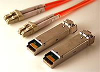 Many system designers are choosing to use pluggable I/O interconnects, including SFP+ and QSFP+, which provide both copper and fiber options. These modules offer high-speed I/O as well as increased port density.
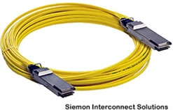 Active optical cables, which mate with traditional copper I/O connectors, offer another alternative. Electrical signals are converted to optical pulses within the connector body, which are propagated through fiber cable. Active optical cables add a degree of configuration flexibility in existing installations. Active optical cable assemblies are available with standard SFP+, QSFP+, CXP, and CX4 connectors.
At 25 Gb/s, it may be difficult for copper backplane interconnects to reach the one-meter, preferred channel length target without the use of exotic PCB materials, advanced signal conditioning silicone, and greatly tightened manufacturing tolerances, all of which add cost. These limitations will continue to open new opportunities for the use of fiber both inside and outside of the box.
Efforts to determine how the advantages of FO links can be utilized inside the box have been under investigation for at least 15 years. A variety of backplane concepts that featured embedded light pipes have been proposed. Optical signals generated on daughtercards would be channeled down to the surface of the PCB, where they would be directed 90 degrees into an optic plane. Unique backplane connectors would conduct the optic signal across a pluggable interface. Optical links embedded in the backplane would direct high-speed signals to the appropriate daughtercards. Other concepts embedded the electro-optic conversion into the backplane connector, which allows the use of conventional copper-based daughtercards. Again, added costs, additional risk due to the introduction of new technology, and the lack of a compelling application have kept these concepts in the development lab.
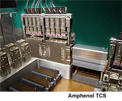 Several connector manufacturers, including Amphenol, Molex, and TE Connectivity, have introduced optical interconnect systems designed to facilitate the use of discrete optical transmitters located on the daughtercard. A pigtail fiber from the transceiver is passed through a conventional backplane to a mating optical connector with an optic loop to another board slot. These physically large transceivers and proprietary connector systems have tended to be expensive and have seen limited commercial acceptance.
More recently, advances in miniaturized optical transmitters, as well as the science of silicon photonics, are presenting opportunities to bring cost-effective optical links inside the box.
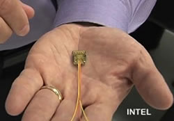 About two years ago, Intel announced its LightPeak optical I/O interface, with a bi-directional bandwidth of over 10 Gb/s. It remains in the lab, while its copper Thunderbolt sister product has been implemented into a number of Apple-related products.
A series of new optical interfaces designed for high-speed applications inside the box have entered the market.
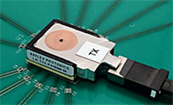 Reflex Photonics introduced its PCB-mounted LightABLE optical engine that mates with an MT-terminated ribbon fiber connector. Each of these low-profile modules provides 12 transmit or receive channels at up to 11.2 Gb/s. The module is surface-mounted via BGA attachment. The Light On Board concept is designed to support optically enabled ASIC packaging by mounting active devices and LightABLE optical engines on the common substrate.
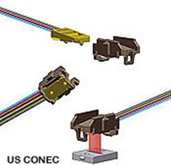
The PRIZM LightTurn connector from US Conec is a miniature separable ribbon fiber connector designed for applications that utilize high-speed parallel optical transceivers. The unique housing provides accurate pre-alignment as well as keying and latching. Suppliers, including Molex and Timbercon, now offer custom cable assemblies using the PRIZM LightTurn connector.
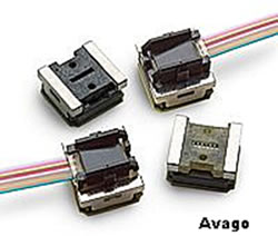
Avago, a leader in fiber optic interfaces, introduced its MicroPOD and MiniPOD parallel optical transmitters, which provide 12 channels, each transmitting at more than 10 Gb/s over ribbonized fiber optic cable. MicroPODs are only 8.2mm x 7.8mm and designed for direct solder or LGA socket attachment to the PCB.
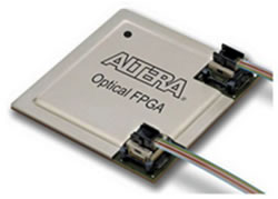 Altera, a manufacturer of embedded processors, ASICs, and FPGAs, announced the first optical FPGA featuring the Avago MicroPOD optical interface. The result is a 12-channel link between devices with an aggregate bandwidth of 150 Gb/s. Questions have been raised about these connectors interfering with heat sinks, but the concept of direct chip-to-chip optical links is appealing.
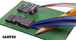 Samtec has entered this market with their FireFly micro flyover system, which allows a designer to choose either copper or fiber interfacing to a common PCB connector. The copper option utilizes 38 AWG ribbon coax cable, while the fiber version includes a miniature optical engine with an integrated heat sink. Both provide up to 28 Gb, bidirectional, protocol-agnostic transmission. The PCB connector can be mounted on a daughtercard or directly on a semiconductor package to minimize PCB trace losses. Applications include chip-to-chip, board-to-board, and system- to-system interconnections.
High-speed communication between chips on the same board can become a performance bottleneck. Copper links experience dielectric attenuation, as well as via structure reflections, skew, and frequency-dependent crosstalk. As system speeds continue to increase, this problem will only grow worse. Silicon photonics enables the integration of electrical and optical elements on the same chip. Building optical components on the common silicon substrate allows fabrication of advanced electro-optical chips using conventional chip manufacturing processes.
IBM and Intel have developed hybrid silicon optical devices that operate at up to 40 Gb/s. The objective is to increase the bandwidth of chip-to-chip communication by transitioning from electrical to optical signaling on the same chip. These development projects are focused on hybrid photonic devices fabricated on silicon substrates, the base of most current integrated circuits. Except for the vertical-cavity surface-emitting laser (VCSEL) light source, all elements of the optical transmitter and receiver are integrated at the wafer level.
IBM recently announced the ability to fabricate optical and copper structures on the same die. This opens the possibility of powerful processors that feature optical I/O using conventional manufacturing processes. Research is being done with the objective of creating direct high-speed optical chip-to-chip communication channels. Cisco systems recently joined the ranks of photonic IC developers with a prototype chip that integrates a laser, an optical lens, multiplexer, and a CMOS modulator. Additional optical communication specialists working on integrated photonic devices include Aurrion, Kotura, Luxtera, and OneChip Photonics. Advances in silicon photonics may provide the technology to eventually usher in true photonic computing.
New applications for fiber optic links inside the box continue to pop up. There have been several recent articles written about interest in implementing PCI Express Gen 3 via optical cabling. Huge potential exists as networks evolve to 40 and 100+ Gb/s data rates. Initial applications would likely appear in enterprise equipment, but could eventually expand into the vast market for consumer products.
Dow Corning and IBM recently announced the development of a new flexible polymer material that can be fabricated into optical waveguides using conventional printed circuit board manufacturing techniques. It is possible that we may start seeing optical backplanes in high-end systems within the next five years.
Broad adoption of on-chip optical interconnects may be the next disruptive technology to shake up the market, but is likely many years off. In the long haul, photon-based computing, if ever realized, could revolutionize the industry. In the short term, miniature active optical cable assemblies now entering the market may offer a cost-effective alternative to copper for interconnection within the box.
- Optics Outpace Copper at OFC 2024 - April 16, 2024
- Digital Lighting Enhances your Theatrical Experience - March 5, 2024
- DesignCon 2024 in Review - February 13, 2024

