Strategic Connector Selection Optimizes Electromagnetic Compliance
Minimizing Electromagnetic Compliance (EMC) is a challenge for designers of digital systems who must pass FCC system tests for radiated emissions. The study of radiated electric field pattern simulations, often used for antenna analysis, helps evaluate the radiation properties of individual interconnects and aid in the selection of properly shielded products.

Electromagnetic Compliance
By Alan Kinningham, Signal Integrity Design Team Manager; Adam Nagao- Signal Integrity Engineer; and Travis Amrine, Global Industry Marketing Manager at I-PEX Connectors
In 1976, the United States Federal Communications Commission (FCC) began addressing radiated emissions in CFR 47 Part 15, Subpart B, covering unintentional radiators. In this section, any digital signaling involving a timing signal in excess of 10 kHz was required to meet limits for radiated emissions. There were (and still are) two classes of devices whose radiated emissions are regulated by the FCC: Class A Devices intended for commercial use, having somewhat tight limits for radiated emissions, and Class B Devices marketed for consumer use, having less rigorous limits.
At first glance, that notion that the FCC would monitor the resolution of a flat panel display or how fast a computer’s CPU processes information might seem strange. However, when one considers that modern digital signals operating at multi-gigabit data rates will cause time-varying electric and magnetic fields to propagate into the surrounding area, it makes a lot more sense. The FCC ensures that the electromagnetic frequency spectrum is properly allocated, protected, and regulated to avoid disruptions to over-the-air communications (i.e., radio, TV, mobile phones, satellite, terrestrial point-to-point, etc.).
The entire spectrum is carefully allocated, guarded, and licensed to the broadcasters of their allotted frequency bands. As electronic devices, communications techniques, and applications for data continue to advance, the FCC’s job of guaranteeing bandwidth availability and compatibility for all users, within their respective bands, is increasingly difficult. Regardless of their designed purpose, many high-speed digital devices will also become unintentional radiators — that is, these devices use radio frequency (RF) electrical signals or sends radio frequency signals over conducting cabling to other equipment, but they are not intended to radiate radio frequency energy. The presence of these signals potentially compromises the proper use of the electromagnetic spectrum to which other communications channels have been assigned.
The FCC first addressed the matter of unintentional radiators from devices such as the Apple II personal computer of the 1970s and the subsequent IBM PC. Today, the explosive growth of data centers, 5G wireless, IoT devices, cloud connections, high-resolution video, and automotive electronics with their accompanying thirst for bandwidth, challenge the ability of devices and components to maintain an atmosphere of electromagnetic compatibility.
Additionally, extreme miniaturization and cost containment must be balanced with aggressive electrical performance to achieve optimum solutions for the OEM and end-users. Higher and higher data rates place greater demands on the need for shielding components, while manufacturers simultaneously work to drive down costs in a shortened product life-cycle environment. Today, to alleviate confusion for designers of high-end systems, specifically mmWave and multi-gigabit applications for a wide variety of applications in 5G, video display, and hand-held device markets, shielding components are often a non-optional part of everyday electronic design.
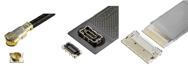
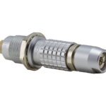
ZenShield® from I-PEX (l to r: MHF®7S RF Coaxial Connector, NOVASTACK®35-HDN Board-to-Board Connector, and EVAFLEX®5-HD FFC/FPC Connector) is a small connector series offering high-performance EMC shelding, which allows board designers more flexibility for designing the board by allowing the connectors to be placed in close proximity to sensitive subsystems, such as transmit/receive antennas, that are commonly found in high-performance wireless communication systems.
Radiated Electric Field Emissions
For the FCC and other EMC regulatory agencies, the topic of electromagnetic compliance addresses radiated emission limits for the entire computer or device. Since a digital electronic system is composed of numerous components, a single, unshielded component has the potential to be the weak link that allows electromagnetic radiation to propagate in excess of the allowable limits, thereby causing the entire system to fail regulatory EMC testing.
Two methods for evaluating shielding effectiveness of a component are full-wave electomagnetic simulation and an indoor shielded anechoic chamber.
Full-wave electromagnetic simulation is performed using a 3D field solver software tool such as the Ansys HFSS (high-frequency structure simulator) or CST Micro-Wave Studio. In these simulation environments, a 3D mechanical model of the connector pair is imported into the simulator and mounted to a cable, PCB, or other transmission line structure in a way that most represents its intended use case. Simulation ports are defined at appropriate points in the accompanying transmission line structure or, perhaps, on the input contacts of the connector itself. The output contacts are attached to a short length of transmission line structure (coaxial, PCB, flex circuit, etc.), and terminated in the transmission lines characteristic impedance. The various electrical conditions, such as frequency range, step size, signal amplitude, and boundary conditions are then set in 3D solver prior to meshing and iterative solving of the resulting fields associated with the structure. For EMC analysis, radiated E-Field emission is a common metric for analysis of shielding effectiveness.
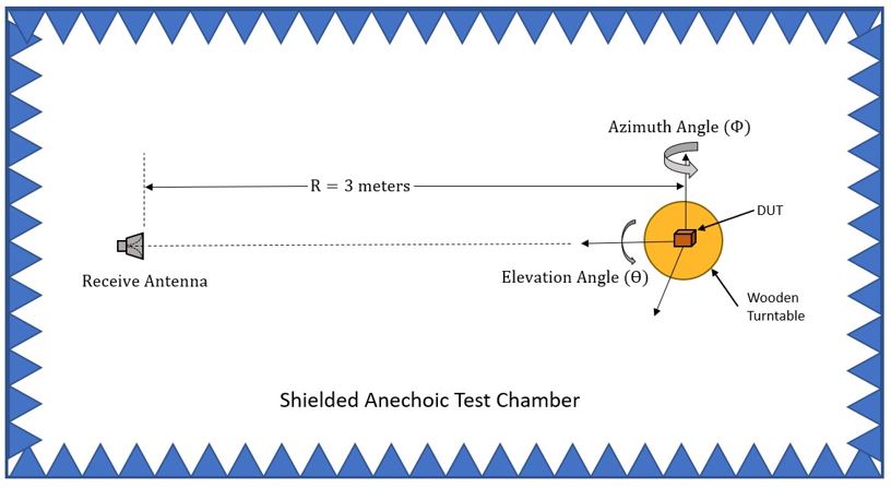
An indoor shielded anechoic chamber is basically a large metal box with a metal door that properly seals electrically when closed. The room (or chamber) has a non-metallic turntable for positioning the device under test (DUT), a receive antenna and appropriate transmission line fixturing, and is used for the measurement of radiated emissions from the DUT. In the case of a passive DUT, a coaxial input cable is run from a signal source outside the room through wall-mounted bulk-head coaxial connectors to produce a signal within the DUT. The DUT is then configured with a shielded termination load to eliminate any excess transmission line reflections back through the DUT.
Advantages of this method are that these chambers are commonly in use for measurement of cellular OTA (over the air) testing and the indoor ranges are usually calibrated for their equivalency to an Open-Air Test Site (OATS). OATS data was originally required by the FCC for Part 15, Sub-Part J compliance purposes.
In this test, the DUT is mounted to the appropriate transmission line (TL) structure and terminated in the characteristic impedance of the TL. The input line is powered by a signal generator. While signal power is applied to the DUT at the appropriate frequency, the turntable sweeps the DUT (or the receive antenna). Any emissions are detected by the receive antenna and conveyed to a spectrum analyzer or power meter. This is commonly done for shielded and unshielded connectors to determine the shielding effectiveness of the connectors’ shielding method.
Read I-PEX’s complete Maximum E-Field Radiation analysis of its Zenshield connectors in the original white paper.
Like this article? Check out our other articles How to Specify connectors, Standards, Sensors and Antennas and our 2022 Article Archive.
Subscribe to our weekly e-newsletters, follow us on LinkedIn, Twitter, and Facebook, and check out our eBook archives for more applicable, expert-informed connectivity content.