Signal Integrity: More Important than Ever
The process of ensuring signal integrity is not a precise science. Even the tiniest nuance anywhere along a channel can cause reflections, crosstalk, or prohibited levels of emitted radiation.
A long time ago in a galaxy far, far away, designers of high-speed digital circuits could quickly verify performance by building a physical “breadboard” prototype. Engineers had a reasonably good chance that the circuit would work in production. The primary concern was to ensure that interconnects offered sufficiently low DC resistance.
Then along came megahertz channels.
Copper channels operating at a certain rise time fundamentally change their electrical characteristics by behaving like transmission lines. Unlike a pair of positive and negative conductors delivering power to a load, a transmission line consists of two conductors that deliver energy in the form of an electromagnetic field.
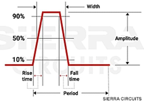
Rise time refers to the time it takes for a signal to transition from one level to another and is a critical factor in achieving signal integrity. As data rates accelerate, the number of positive and negative transitions per second increases, which results in shorter rise and fall times. The result is an increase in high-frequency components that are susceptible to distortion. Designers began to recognize the transition to transmission lines when clock rates approached 50 Mhz.
Applying signal integrity regimen started to become important when rise times fell below 1 nanosecond, and mandatory at rise times less than 200 picoseconds. Today, the rise time of a 200 Gb per lane Ethernet signal is only ~35 picoseconds. The industry is now in the process of evolving to 200 Gb/s lanes while AI is pushing data center networks to 1.6 Tb, increasing the necessity and challenge of ensuring signal integrity a process that has become standard practice in the new product design cycle.
Nearly every element of a transmission line influences performance. The type of insulation and spacing between conductors become critical factors. The precise geometry of how differential conductors in a printed circuit board are related to each other, and to a ground plane, influences performance. This phenomenon requires an entirely different approach to high-speed circuit design, especially in an era where system reliability and meeting time-to-market objectives are imperatives.
All sorts of bad things happen to poorly designed circuits. Reflections resulting from changes in impedance anywhere along the circuit can distort the signal and can be generated by connectors, via holes, stubs, and even sharp turns on a PCB trace. High-speed copper channels today are carefully designed to maintain a consistent 85W (ohms) to 95W impedance. Failure of a receiver to detect a signal may be traced to a low signal-to-noise ratio. Simple attenuation may lower the signal level to undetectable levels. Jitter refers to the deviation of a signal’s timing from its ideal position, a condition that can cause errors at the receiver. Intersymbol interference is the result of “smearing” of signal pulses that reduce the ability of the receiver to distinguish individual symbols. External devices or nearby circuits in today’s high-density packaging can generate electromagnetic interference (EMI) that can result in noise and crosstalk. Lower voltage swings and reduced noise margins make signals more difficult to detect. Increasing data rates over longer circuit lengths amplify these negative effects and can limit the length (reach) of high-speed circuits. A general rule of thumb predicts the practical reach of a transmission line is halved as data rates double.
Signal integrity is all about anticipating these factors, compensating for them, and verifying channel performance before a problem gets baked into the final design. Achieving signal integrity requires an integrated process of simulation, analysis, and design adjustments to mitigate transmission issues. Doing this very early in the design phase allows a series of design rules to be created that dictates the layout process. This is accomplished through a process of computer simulation and testing, to identify the sources of noise, loss, and distortion. This process enables the ability to test the effect of circuit changes in real time to achieve optimum performance. Once a computer model performs well, testing the circuit in the anticipated environment confirms the ability of a design to work in the production product. The greatest value of verifying signal integrity is that it is a form of risk reduction. Introducing a new product into the market entails plenty of risk; eliminating as many potential sources of failure as possible is a strong incentive to a project manager. The ultimate objective is to get it right the first time.
One example of an effort to support ever-higher data rates was the industry transition from non-return to zero (NRZ) modulation to pulse amplitude modulation 4 (PAM4).
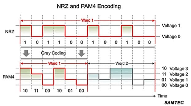
Rather than double the bandwidth of a channel that would increase SI issues, PAM4 modulation doubles the number of bits transmitted per cycle, increasing efficiency of the channel.
A significant tradeoff of using PAM4 modulation is reduced margin for noise. As the number of bits per symbol increases, the threshold gets smaller, resulting in reduced noise immunity.
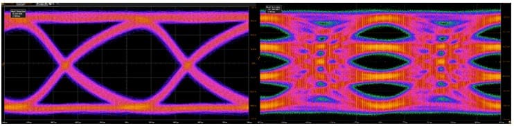
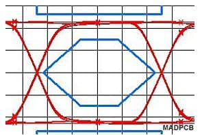
Eye diagrams of NRZ and PAM4 circuits illustrate the challenge of using PAM4 modulation, requiring even tighter control of all circuit parameters. PAM4 modulation has been broadly adopted for high-speed channel design with interest growing in PAM6 or PAM8 modulation.
Developers have adopted several strategies to overcome the challenges of PAM4 signaling including forward error correction (FEC) and decision feedback equalization (DFE). FEC adds redundant data to the bitstream and uses algorithms to ensure that the receiver can reconstruct the data, reducing the bit error rate. DFE amplifies select components of a high-speed signal without boosting noise, which can compensate for intersymbol interference. Both technologies add complexity to the channel and may result in increased power consumption latency and unwanted generation of heat but are widely used to help maintain signal integrity.
 Design engineers have a great amount of flexibility when choosing the laminate material and laying out a high-performance PCB circuit, but little control on what happens to the signal when it passes through a connector. As data rates increased, connector manufacturers responded by changing the physical arrangement of contacts from a standard open grid to shielded differential pairs.
The internal geometry of connectors was upgraded to maintain a constant impedance through the interface. Some suppliers utilize several different plastic materials in a connector to reduce reflections. The PCB launch footprint was optimized by reducing the diameter of the plated through hole, and back-drilling to eliminate a reflective stub. In some cases, through-hole PCB termination was replaced with surface mount contacts. In addition to supplying 3D drawings and extensive SI support, leading manufacturers now provide high-speed connector models that a user can plug into their channel simulations. They may also loan or sell test PCB boards that allow a user to physically test a circuit using a variety of parameters. Recognizing the importance of maintaining a consistent signal path, connector manufacturers collaborated to provide mechanical and electrically identical competitive connectors to ensure plug compatibility among second sources.
Modeling and simulation of circuits require advanced test equipment and software as well as skilled technicians who can interpret test results and make appropriate circuit changes. A variety of criteria are applied to establish and verify signal integrity. Circuit analysis can include simple checks for impedance discontinuities or radiated emissions. Channel characteristics, including bit error rates, are a key measurement of the ability of a channel to deliver data with minimal errors. Eye diagrams provide a rough indication of signal quality. S-parameters are used to debug and validate design. Channel Operating Margin (COM) establishes the lowest level of acceptable performance and provides a measure of confidence that a channel will perform to a specific specification.
The equipment required to perform SI analysis and verification is not for the shallow of pocket. An SI engineer needs access to:
- High-bandwidth sampling oscilloscope to view eye-diagrams
- Time domain reflectometer to locate impedance discontinuities
- Extensive suite of advanced simulation and modeling software.
- Vector network analyzer, to measure S-parameters and analyze channel frequency response
- Bit error rate tester (BERT) to count channel errors at the receiver
- Signal generator to simulate and characterize a channel
- A collection of test fixtures and probes
A high-end benchtop vector network analyzer can have a $1 million price tag.
Today, best design practices to achieve signal integrity are implemented at the start of a new product design cycle. The process of ensuring signal integrity is not precise science and is still considered somewhat of a black art. Even the tiniest nuance anywhere along a channel can cause reflections, crosstalk, or prohibited levels of emitted radiation. There is no universal cookbook that will guarantee success. Eric Bogatin, a recognized signal integrity guru, said There are two kinds of designers: Those who have signal integrity problems and those who will.” He has published a series of rules and guidelines that point a designer in the right direction.
Attaining a level of signal integrity that allows a circuit to work the first time has never been more challenging or more essential to the successful launch of a new electronic device.
Visit Bob Hult’s Connector Supplier archives to read his ongoing coverage of high-speed advancements and see his show reports, including DesignCon 2025 and OFC 2025.
Like this article? Check out our other Radiation and Signal articles, our Military and Aerospace Market Page and our 2025 Article Archives.
Subscribe to our weekly e-newsletters, follow us on LinkedIn, Twitter, and Facebook, and check out our eBook archives for more applicable, expert-informed connectivity content.

- XPO, Addressing the I/O Panel Bottleneck - June 30, 2026
- Agentic and Neuromorphic Computers Enable the Future of Digital Computing - May 26, 2026
- OFC 2026: High-Speed Networking in the AI Era - April 7, 2026