How to Prevent EMI When Designing an Interconnect Solution for Medical Devices
Electromagnetic interference poses a threat to product functionality as well as patient health. The right shielding architecture can help avoid it.
By Zachary Blanden, Industrial Engineer, Nicomatic LP
EMI, or electromagnetic interference, is a branch of EMC, which stands for electromagnetic compatibility. EMI refers to the study and mitigation of interference of noise signals to keep them from impacting a given circuit’s receiving (immunity) and transmitting (emission) functions. In the medical world, creating sufficient signal noise barriers is imperative to optimal device functionality and ultimately protects patients’ health.
A good EMI shield can be thought of as a full 360° enclosure surrounding the protected devices. A full 360° shield is a circumferentially terminated electrical termination that surrounds the entirety of the protected device (e.g., cable) and connects it to a chassis (See Figure 1).
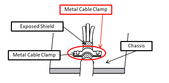
Full 360° grounding[1]
In certain medical applications, this is seemingly unachievable because the device that needs protection is a transducer, which is a sensor that transforms physical phenomenon into electrical signals. For example, the desire to shield a phototransistor used to measure the translucency of a certain abnormality within human tissue, given a light source behind it, in order to protect it from outside interference and avoid damaging the circuit or hindering its functionality is reasonable. But how can such a device be shielded? Completely wrapping the phototransistor in metal foil would eliminate the sensor’s ability to pick up light, and there are a plethora of other medical sensors — light, temperature, pressure, flow, heat, acoustic, and more — that also require shielding that allows certain stimuli to pass through.So, what can designers do? Early attempts at providing effective shielding for applications like these consisted simply of surrounding the desired circuit with conductive material, but without a grounding methodology. This solution, though not specifically related to medical sensors, is called a floating shield.
Ultimately, this is a problematic design. Floating shields add extra metallized layers of shielding materials to surfaces, without proper termination, to protect circuits from incoming noise signals while simultaneously preventing outgoing noise signals. However, supplementary metalized layers or structures without sufficient termination will create two independent pieces of metal, typically the shield and the chassis, and thereby create a dipole antenna, which has the potential to convert a field into a voltage and current. This could cause both circuit immunity problems and compromise shield performance.
To avoid floating shields, designers often incorporate drain wires, which they use to connect the independent pieces of metal, eradicate the dipole antenna concern, and establish electrical unity, usually through a shield to chassis connection. However, drain wires, sometime referred to as pigtails, induce other EMI issues.
The addition of a drain wire creates a mutual inductance loop between outside noise and inside circuits, hindering shielding performance. Drain wires also force a high current density by focusing electrons exclusively on the pigtail terminations, which allows voltage buildup between the cable shield and the mating enclosure (e.g., chassis). In turn, a current will develop and either generate outward signal, causing radiated emission problems, or impact the internal circuitry, causing immunity problems.
One common solution to this pitfall is to use internal cable conductors as the ground path for the internal ground by connecting the shield directly to a specified conductor, but this is more common in flat cables than round wires. Further, doing so doesn’t actually solve the inductance loop problem; it just repositions it. However, a grounding conductor is still a valuable asset to shielding if the cable shield also has a 360° connection to the chassis, as it is important to minimize the loop area to mitigate the inductance it creates. Without a fully enclosed 360° termination connection, the electrical signals cannot differentiate between the outside world and inside circuitry, which again creates emission and immunity problems.
By now, it is clear that a full 360° degree closed conductive surface is the most effective way to shield devices and cables. Figure 2 illustrates an ideal shielding scenario. This type of situation creates a complete and distinctive barrier between the inner circuitries and outside noise signals. However, as noted, this best-practice shielding solution can sometimes be impossible to implement due to medical restrictions for end-sensors or probes.
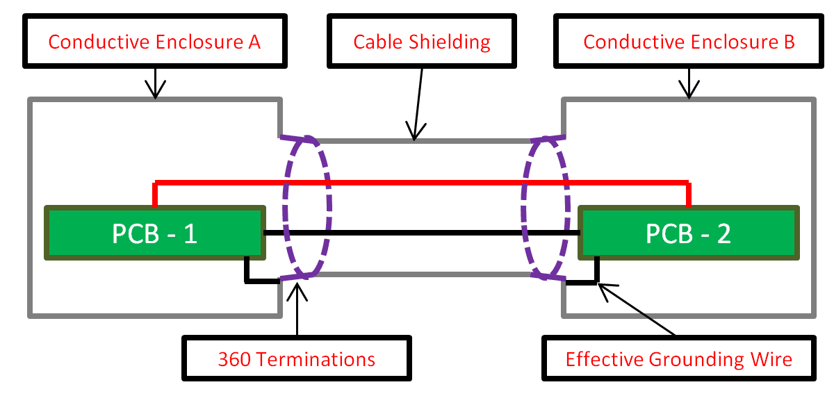
An ideal shielding scenario
So, what can be done to effectively protect a device from outside noise signals while simultaneously allowing external stimuli to produce and transmit electrical signals? There is a well-established mathematical relationship for closed conductive surfaces to the size, number, and spacing of perforations (i.e., through-holes). When properly executed, these perforations, which are much smaller than a wavelength, will still provide sufficient EMI protection while allowing certain types of stimuli through. Additionally, extremely thin layers of conductive coatings can sometimes be translucent enough to allow certain types of signals, such as light, to pass through while still providing effective EMI shielding.
This relationship has been studied and defined as:
- N = number of round or square through-holes
- a = diameter or edge size of the through-holes[2]
Where spacing between the “a”s is minimal [a/10], EMI ~Na3, and EMIdb ~20 Log(Na3). (See Figure 3 for a visual representation of this relationship.)
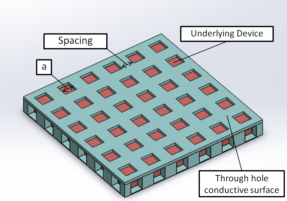
Conductive surface with through-holes for EMI protection
Though this holds true, it is still important to completely terminate the perforated conductive surface via full 360° terminations.
In summary, the ideal shielding solution would be to completely surround a circuit with a seamless conductive enclosure. However, since this is impossible — especially in medical electronics, like transducers, that require both EMI shielding plus the ability to allow certain stimuli to pass through — design engineers have attempted to properly terminate shields using a multitude of methods. Typical grounding methodologies have several glaring flaws, floating shields create dipole antennas, drain wires create interfering inductance loops, and, unless their shields are properly terminated, internal conductors eliminate a system’s ability to differentiate between the outside world and inside circuitry. This iterative process has ultimately resulted in EMI solutions comprised of very thin layers of closed conductive materials with extremely small perforations (<λ/20, and closer to λ/50) and 360° fully shielded cable-to-chassis connections. This type of shielding can be used for medical electronics with relatively high frequencies of approximately 2.5GHz.[2]
Though supplementary challenges and barriers will often arise when attempting to shield medical devices, avoiding classic pitfalls and employing well-researched shielding architecture solutions can help create effective shields for nearly all of these problematic applications.
References:
- Image. https://www.focusondrives.com/wp-content/uploads/CableShieldingGood.jpg
- Hill, Lee, “Mechanical Design for EMC.” Electromagnetic Compatibility Workshop. Westford Regency Inn, Westford, MA. May 15th and 17th. Lecture.
Interested in a specific market? Click a market below for current articles and news.
Automotive, Consumer, Industrial, Medical, Mil/Aero, Datacom/Telecom, and Transportation


![]()