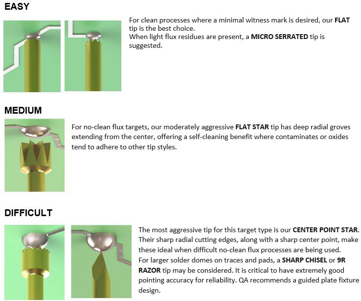
Selecting Test Probe Tips to Test Printed Circuit Boards
Printed Circuit Boards (PCB) are an essential part of the many electronic products we rely on every day. Both in-circuit and functional testing after manufacturing are critical steps to ensuring PCB dependability. Test probes play an important part in this process by providing the flexibility to make the electrical connections between the test system and the vast variety of contact points typically found on PCBs.
While there are many factors that affect a probe’s ability to make reliable electrical contact, proper tip style selection is one of the most important. Incorrect tip selection could cause false failures where no defects are found (NDF), lower your first pass yields (FPY), or in extreme cases, damage the unit under test (UUT). Selecting the right tip can reduce the overall cost of test by increasing the output of units being tested and extending the life of your test probes.
Test engineers often have different experiences as to which is the best probe tip style for a given contact surface. The following considerations will help you select the right tip style for many of today’s common test targets.
Test target types
It is important to consider the size, shape, and other features of the test targets. There are various PCB targets such as pads, vias, leads, posts, and solder bumps, which range in probe-ability from easy to difficult.
Board manufacturing processes
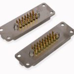
Tip materials
Tips are made from either beryllium copper (BeCu) or steel. Both are gold plated over nickel. Steel, while harder than BeCu, will have reduced wear and remain sharp longer, but has a higher bulk resistance.
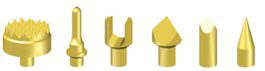
Test probe tip geometry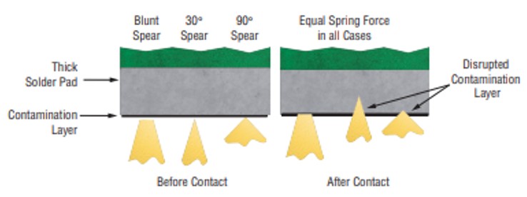
There are many different tip styles, each with their own unique geometry. Tip geometry and sharpness will determine the ability to penetrate contamination layers. A tip that is blunt or has dull edges will make contact over a larger area thus reducing its ability to penetrate contamination layers on the test targets. A tip that has a sharp point or steep cutting edges applies a higher pressure against the solder causing it to yield. As the solder yields, any oxides or remaining flux residues are disrupted, allowing better electrical contact.
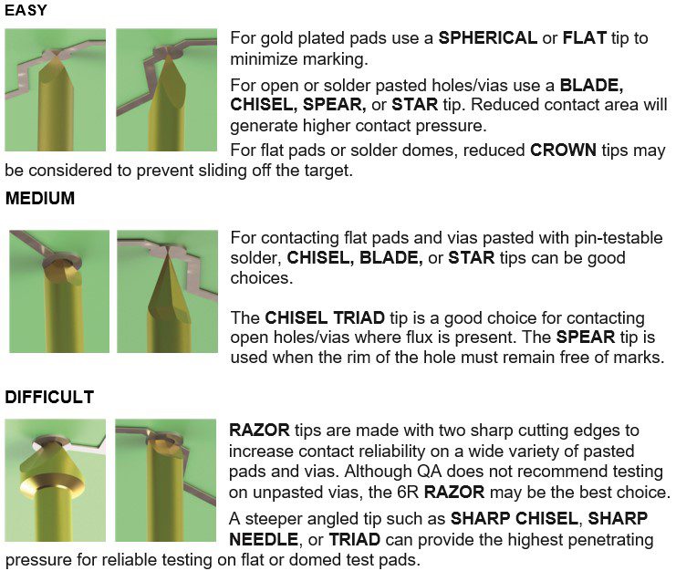
Recommended tip styles for target types
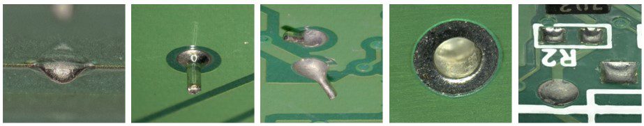
Test pads, vias, and through-holes come in a wide range of sizes, surfaces, and shapes. They can be solder pasted, unpasted, concave, flat, or convex (dome).
Vias and through-holes in a PCB are typically used to pass a signal from one layer to another. When these are to be used as test points, it is necessary that they are not solder-masked so that they can be easily probed.
Leads and Posts 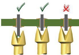
A lead is a terminal on a component. They could be different lengths, straight or bent. Smaller leads will require tip styles with closely spaced cutting edges to trap the leads. A post is larger in diameter and more rigid than leads.
Multi-point tips are designed to capture a target, such as a lead or a post. Some styles have steeper valleys between the tips, creating a self-cleaning feature where it allows contamination to escape.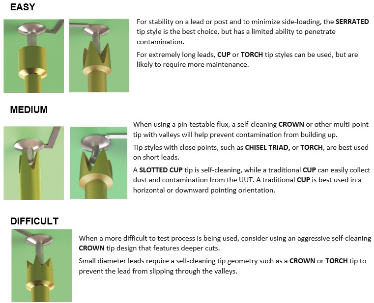
SOLDER BEAD/BUMP/DOME
BEAD/BUMP/DOME technology provides test point accessibility by placing an excessive amount of solder on traces to create a round dome of solder in order to be probed. There are a variety of tips designed to contact differing bead/dome profiles.
In addition, there are many specialty tip styles for other important, but less common applications.

 Other applications for test probes, such as the connection points between the universal test system and the dedicated test fixtures, are outside the test fixture. When used in this application, the test probes are mounted in the test systems “receiver” on a standard grid pattern that mates with either posts or pads on the bottom side of the fixture. The test probes used in these applications have special tip features and are specified by the test system manufacturer.
Other Considerations
- When new fixtures are built, verification of the selected tip styles once all board elements are identified must be performed. Initial processes and solder types can vary from the prototype PCB design to the production boards. In preparation for the launch of production UUTs, tip styles may need to be changed to a different geometry or a more aggressive style based on the cleanliness of the board.
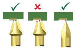
- If the tip style recommendations do not generate good electrical contact, look closely at the witness mark that the probe tip should have made on the test target. Poor pointing accuracy, TIR of the probe assembly, as well as the diameter of the target can be attributed to missing the intended target. While certain tip styles may work well on flat or concave vias, when a dome is present, and pointing accuracy is not good, they may glance off the target and hit the solder mask.

- If your board process causes the solder mask to be below the test point, a multi-point tip may work even if you do not have good pointing accuracy.

- If your solder mask is higher than your target, one or more of these multipoint tips could prevent the others from making electrical contact. In this scenario, change to a single point probe to hit the target.
- In cases where you cannot improve the pointing accuracy on leads or posts, select a larger diameter tip style to maximize the ability to hit the test target reliably.

In situations where the proper tip style has been selected but contact is still not reliable, it may be necessary to evaluate other spring force options. For example, a change in solder paste chemistry may have the unintended consequences of a more difficult to probe surface requiring the use of the next higher spring force in order to maintain the same production rates.
In summary, it is critical to select a tip style with the right number of points of contact, the correct angles, and sharpness. Improving the electrical contact to your test targets will help increase probe life and improve your FPY. Higher yields mean less time troubleshooting false failures, faster through-put, and ultimately, lower overall cost of test.
Leah Hudson has been a Product Design Engineer with QA Technology Company Inc. since 2017, designing specialized spring-loaded test probes and hyperboloid contacts for a multitude of industries and applications. When new products aren’t on the agenda, you can find her working with applications engineering, answering customer questions, and improving upon existing product offerings.
Matt Parker is an Applications/Product Design Engineer at QA Technology. Since the late 90s, he has been educating customers in the application of testing PCBs and products through the use of spring-loaded test probes and their related sockets. Other functions include failure analysis and product testing for customer supplied probes with the effort to improve first pass yields while increasing probe life.
To learn more about tip style selection, visit QA Tech.
Like this article? Check out our other How to Specify articles and our 2024 Article Archive.
Subscribe to our weekly e-newsletters, follow us on LinkedIn, Twitter, and Facebook, and check out our eBook archives for more applicable, expert-informed connectivity content.