Chip Technology Struggles to Keep Pace with Moore’s Law
The technical challenges of designing and building devices that pack tremendous computing power into tiny packages are considerable. But new high density semiconductor technologies offer a path to keeping Moore’s Law alive.
For nearly 60 years, Moore’s Law has set the pace of advancements in semiconductor chip density, but a combination of physics and economics is altering the strategy by which next-generation devices are being designed and fabricated.
A continuous process of shrinking node geometries has enabled incredible advances in system performance. More nodes per unit area increases the capacity and speed of a chip. Shorter electrical paths on the die minimize latency and power consumption. Today we have commercial production chips that are built on a 14 and 10 nanometer (nm) process. High performance chips based on 7 nm and 5 nm have entered the market. TSMC, the world’s leading semiconductor fabricator, is working on a 3 nm process targeting digital signal processor (DSP) applications. Longer range projections are looking at 1.4 nm devices. IBM announced a new 2 nm chip that features 50 billion transistors, each of which is smaller than a strand of DNA.
The technical challenges of designing and building devices at these levels is limited by the ability to manipulate single atoms. Developing new fabrication technologies that can build chips on 1.4 nm requires new imaging and assembly processes that can deliver acceptable failure rates on chips with over a hundred billion nodes. The cost of building a state-of-the-art chip fabrication plant can run to $20 billion. As a result, next-generation chip development cycles are being stretched out to more than three years.
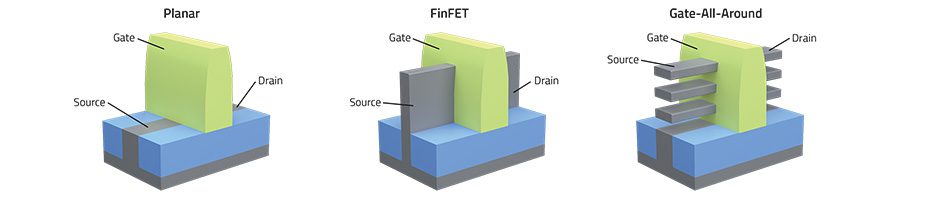
Evolution of planar technology, image courtesy of LAM Research.
Design and fabrication of semiconductors have undergone a continuous evolution over the past 60 years. Planar semiconductor technology has been in use since 1959 and is the simplest to design and fabricate.
FinFET devices feature significantly faster switching times and higher current density than planar technology. FinFET is a non-planar 3D structure that has become the basis for modern semiconductor device fabrication.
GAA (or gate-all-around) transistors are being utilized in 3 nm and smaller geometries. In this chip architecture, the gate surrounds all four faces of the channel, which enables greater control of current flow, resulting in high power efficiency.
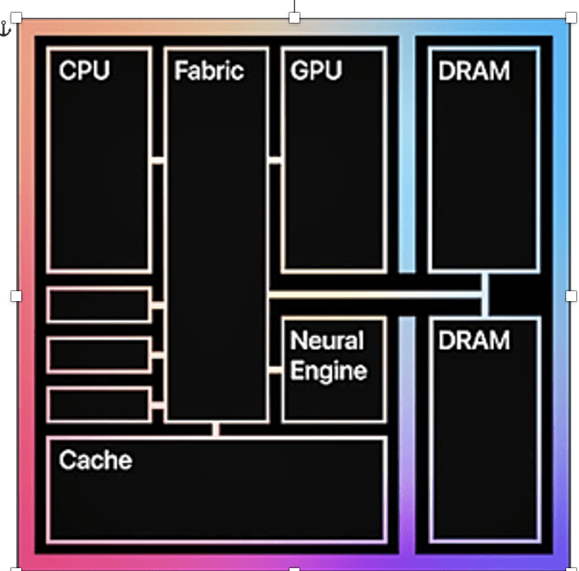
Apple M1 chip block diagram
Complexity of integrated circuits has increased exponentially, often integrating multiple functions, including computation, memory, and communications on a single die.
The Apple M1 chip, for example, featured two processors and eight cores, with 16 billion transistors, a network fabric, as well as cache and DRAM memory.
This type of chip architecture, which combines multiple or high-level functional elements of an electronic device onto a single chip, is defined as a system on chip (SoC).
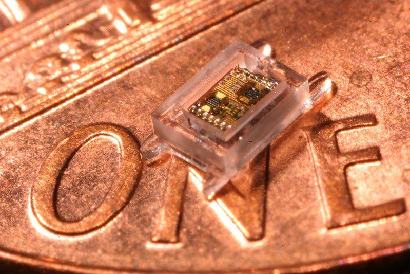
An M3 computer with and without encapsulation. Credit: Electrical & Computer Engineering at the University of Michigan, Ann Arbor.
The ability to pack more transistors in smaller spaces has revolutionized the world of electronic products. Entire computers can be packaged in an envelope not much larger than a grain of rice.
Demand for building even more functionality into a single chip continues, and designers have four options to accomplish this goal.
1. Feature sizes can be reduced, but as we approach 1 nm geometries, increased cost results in diminishing returns on investment.
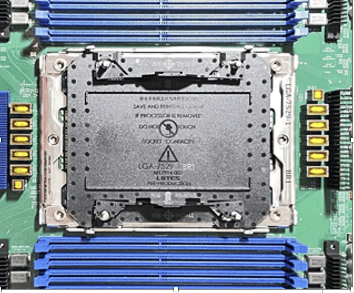
2. The size of the die can be increased, but that reduces the yield from each wafer, and increases the cost of wafer defects, increases power consumption, and consumes more precious PCB space. The massive Intel 7529 processor, for instance, measures 66 mm × 92.5 mm; that is a huge footprint by traditional chip standards.
3. System in package (SiP) bundles multiple integrated circuits and passive components into a single package. Discrete elements are mounted on a common substrate and communicate via copper interconnects. This contrasts with SoC, whereas all functions are integrated into the same die. SiP packaging is particularly attractive when different circuits based on multiple process nodes are required.
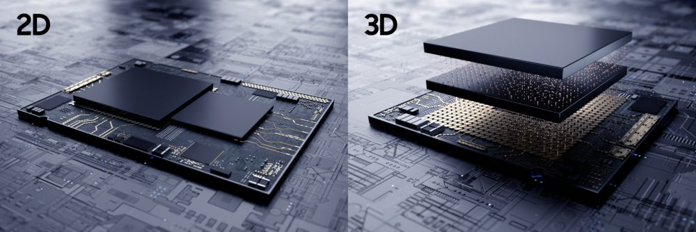
4. Evolving from 2D to 3D structures with vertical stacking of multiple dies is in the process of being adopted and is seen as a path to keeping Moore’s Law alive.
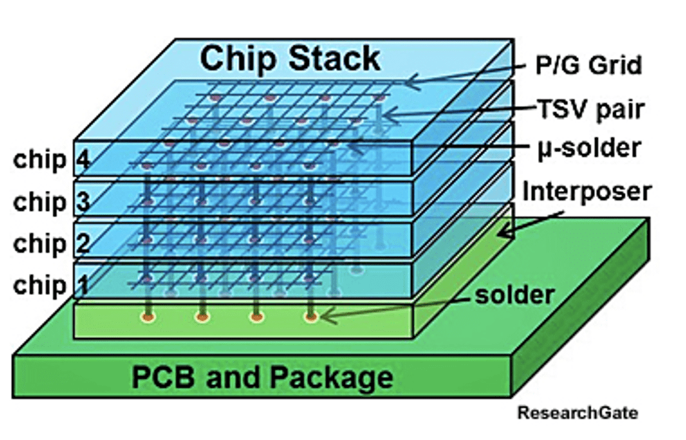
Multiple chips can be stacked and interconnected using through-silicon-via (TSV) links. Entirely different chips such as analog, RF, memory, and optical using different process geometries can be stacked to create highly scalable custom modules. These assemblies are mounted on an interposer that may be soldered or socketed to a host printed circuit board.
Rather than mounting two chips side by side on a substrate, Samsung X-Cube technology enables stacking a memory chip on top of a logic die. This results in shorter high-speed signal paths and greater energy efficiency, while reducing the package’s PCB footprint.
Samsung’s X-Cube
Chiplets introduce a new tool in the design bag of system engineers. Chiplet architecture is based on small footprint sub-assemblies that enable a modular approach to system integration. They are designed to communicate and form more complex integrated circuits. Chiplets provide engineers greater design flexibility and scalability while reducing system power consumption. Design time is reduced, which lowers total development cost.
A relatively new co-package optic (CPO) technology is getting a lot of attention among system designers and engineers. (See this Laser Focus World article for more visualizations.) Driven at least initially by the anticipated high-speed I/O demands of next generation data center switches, CPO offers an alternative to traditional copper interconnects between the switch or any high-speed ASIC and the I/O panel.
Conducting high-speed signals through copper traces embedded in a PCB result in signal loss and distortion as well as increased power.
Using twinaxial cable reduces these negative effects but continues to result in a signal density bottleneck at the 1U I/O panel.
CPO architecture surrounds the ASIC with electro-optic transceivers in a chiplet form factor all mounted on a common substrate. The short electrical path from ASIC to chiplet minimizes copper losses. Optical fibers link the chiplet to the I/O panel where multi-fiber optical connectors provide the required density and signal capacity.
CPO represents a significant change in system architecture and many issues, such as the location of the required laser on the substrate or mounted in a pluggable external module, must be standardized. Other issues revolve around chiplet pluggability, system reliability, and repairability. The current lack of recognized packaging and interface standards is being addressed by the Optical Internetworking Forum (OIF). There is little doubt that next generation 102.4 Tb switches will be challenging and require a rethinking of available system packaging options.
In addition to the technical challenges that are influencing the future direction of advanced semiconductor design and fabrication, political and environmental issues are also impacting the industry.
The race for global semiconductor supremacy is on. While Taiwan remains the source of 90% of the most advanced chips, China and the United States have identified the strategic leadership imperative that high-performance semiconductor design and fabrication represent. Commercial, military, and consumer chips are the lifeblood of everything from advanced weapon systems to coffee makers. Both countries are pouring immense resources into semiconductor research, including design, advanced materials, and human resources. The Chips for America Act approved in July 2022 offers $53 billion to boost domestic chip manufacturing and supply chains. China is investing billions to develop advanced chip technology to eliminate dependance on advanced semiconductors from the U.S. A glaring weakness in the U.S. strategy is the shortage of experienced engineering talent in the workforce as well as in the educational pipeline.
Fabricating semiconductors is an energy intensive process that results in an estimated 0.3% of global carbon emissions. The Semiconductor Climate Consortium consists of a group of 90 companies committed to climate action throughout the semiconductor value chain. The objective is to reduce the IC industry carbon footprint through increased efficiency and use of renewable energy.
Semiconductor design, fabrication, and packaging continues to evolve to address emerging applications. Manufacturers have begun offering single chips and multi-die modules designed for specific applications such as autonomous transportation, machine learning, and quantum computing. Accelerators using optimized custom chips have become an integral element in AI high-performance computers.
Given the imperative and funded commitment to advancing semiconductor technology, it may be a bit premature to mourn the end of Moore’s Law.
Visit Bob Hult’s archives on Connector Supplier to learn more about the technology trends that are shaping our world.
Like this article? Check out our other RF and Coax, High-Speed articles, our Datacom Market Page, and our 2023 and 2024 Article Archive.
Subscribe to our weekly e-newsletters, follow us on LinkedIn, Twitter, and Facebook, and check out our eBook archives for more applicable, expert-informed connectivity content.

- XPO, Addressing the I/O Panel Bottleneck - June 30, 2026
- Agentic and Neuromorphic Computers Enable the Future of Digital Computing - May 26, 2026
- OFC 2026: High-Speed Networking in the AI Era - April 7, 2026