Connector Miniaturization Happens
Over the years, many connector products have been getting smaller, smaller, and smaller. They don’t do this by themselves; miniaturization is caused by electronic systems and subsystems shrinking while being packed with high-density chip-level components.
Many connector systems remain relatively large. This disparity in size is because connector designs are as broad as the electronics and electrical industries combined — from small signal connectors in mobile, handheld, or even medical implant devices, to large, mechanically robust connectors used in high-power, high-voltage applications, computer rooms, electrical equipment, power generation, and electrical distribution. Between these two extremes exist many other various-sized connector designs.
The definition of miniature means different dimensions for different applications. Small form factor connectors, for example, are a separate issue, far beyond this article’s scope. These connectors are generally considered to have ≤ 2mm pitch. High-performance backplane interconnects have migrated to low single-digit mm contacts that support 25-40Gbps operation with scores of contacts. In that application, they are considered high-density. Flexible circuit connectors (FPC) can be very small and have contact spacing as low as .200mm. Ultra-fine pitch connectors generally have pad, beam, or micro-spring-type sliding contacts rather than pins. Nano-Miniature D-Subs are available with pins spaced at .635mm pitch. Area array sockets have contact spacing of 1.00mm or 0.800mm, but up to 2011 contacts/socket. These sockets in the Land Grid Array format (LGA) have thousands of spring contacts instead of pins as well as an equal number of solder balls for SMT attach. All of these designs allow contacts to be accurately spaced; securely anchored in housings or injection moldings; and utilize wiping contacts and other characteristics important to their applications. There are also vertical Z-axis contacts in some applications, which use a variety of custom contacts, including elastomerics and micro-wire bundles.
The miniaturization of connectors is interesting as dimensions approach and may exceed the outright minimums possible with conventional connector technology, raising questions such as:
- Can the connector industry keep pace with micro-miniaturization of equipment technology or will such change be met by disruptive technologies such as silicon micro-machining, i.e. MEMS technology?
- Will extreme micro-miniaturization even happen beyond the scope of existing and future connector capabilities?
- Will design compromises have to be made to achieve cost and reliability factors?
- Will minimum connector dimensions continue to decrease in size with ever-lower mated height, surprising even experts, and meet all future microsystems requirements?
- As seen in the past, with connector technologies surpassing barriers such as Cu continuing to improve versus fiber; Gbits performance vs. Mbits; thousands of contacts thought not possible in a high-volume/low-cost/pin LGA socket; could continuous subminiaturization be possible?
These downsizing pressures have been brought on by Moore’s Law’s progression in semiconductor technology — expected to reach 8nm by the end of this decade. This does not necessarily mean smaller ICs, but more transistors and performance. It also means an entire subsystem or system can be diffused into one chip. IC packaging advances have also occurred with flip chip/C4 packaging, with stacked die packages, and with continual improvements in surface mount technology, chip shooters, etc. of very small devices. Packaging regimes, including 3D packaging of IC devices, have embraced the miniaturization required by modern mobile and handheld devices, while connectors, for the most part, have met their challenges of fine pitch and low mated height. One key aspect of connector use in mobile systems is that many small subsystems, such as radios, SSDs, SODIMM memory, cameras, and LCD displays, are produced by various vendors and must be connected into a single system. But, the pressures are continuing, as seen in trends such as:
 Larger systems giving way to handheld electronics
- Notebooks giving way to thinner and lighter
- SOP to BGA to LGA to MicroPGA to flip chip
- Chip components from 0805 to 0201 (0.600 x 0.300 x 0.220mm)
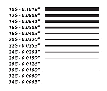
- Wire gauges from 10AWG to as small as 34AWG (.0063” or 0.16mm)
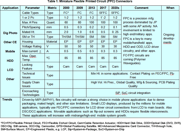
- FPC connectors from 1.00mm to 0.200mm pitch, with mated height from 5.90mm to 0.900mm or less
Sub-miniaturization barriers to conventional connector technology are many, but most are solvable. Many connectors are operator-inserted, designed for 100s of contact cycles, and need varying degrees of robust contact design. Others, typically those in mobile systems, are connected once but need to stay connected through system life, which includes being dropped, vibration, and other environmental factors. Rules of contact reliability require solid contact capture and scrubbing action to avoid corrosion.
Mating force is also an important parameter; higher force means more solid point-to-point contact. Ultra-small contacts may become too fragile for repeated connection cycles; are prone to stubbing failure, burn-out or cross-talk; and could lose contact over time due to stress relaxation and other factors. Cu-alloy stamping processes are advanced but bottom out in fractional mm dimensions, with contact strips requiring special handling during connector molding or assembly. While etched contacts are produced for some very fine pitch applications, their costs are higher. Micro-machined (wet chemistry) contacts are possible, including MEMS-type processes, but so far these have been used only in devices such as micro-accelerometers and in some IC test applications. Micro-machined contacts for test sockets are high-cost items ranging into hundreds of dollars per socket, which is impractical for most production applications.
Interconnects in semiconductor-packaging applications, such as wire-bonds and solder balls/C4, are beyond the scope of conventional connector technology and are usually fixed, rather than demateable contact types. True demateable micro-miniature contacts, say of the MEMS variety, may well be used in future monolithic or robotically assembled micro-systems. Some very small systems, such as in medical implant devices, use mostly high-cost, out-of-mainstream connector designs and applications, or eschew any demateable contacts. In the distant future, IC advances into SiP and SoC will tend to limit separable contact-connectors to intra-system, board-to-board, module-to-board, FPCA, LCD, and to the IO ports of handheld devices.
Stamped or etched contacts encapsulated in an FPC or miniature board-to-board package currently reach .200mm pitch and .900mm mated height. Dimensions below that will include connectors etched into PCBs, use of micro-wires for contacts, or other thin film depositions. Sub-miniaturization of electronic packaging platforms (e.g. HDI, 3D, printed electronics) may force changes in subsystem interconnects or depend on direct attachment of component parts. Thus, requirements below 200µm pitch and 0.500mm mated height may require prototype/experimental interconnect technologies like etched foil or MEMS-type micro-machining.
In the former OEM vertically integrated design and manufacturing model, such as historical PCB and packaging breakthroughs at IBM (or currently at companies like Intel), this kind of technologic leap is possible, but it is less likely today in the global supply chain that includes intermediary board assembly and contract manufacturers. Some EMS providers have capabilities in micro-assembly, evolving from their work on UltraBooks, smartphones, and tablets. These include substantial multi-billion-dollar companies like Foxconn, Celestica, Flextronics, or Sanmina/SCI and Taiwan’s ODM industry. In addition, the semiconductor packaging industry led by ASE, Amkor, and others continually works on subminiature packaging parameters, centered on IC packaging and interconnects.
PCB manufacturing technology has moved to microminiaturization of conductor lines and spaces, as low as 25µm for specially processed, build-up, multilayer HDI printed circuits. 85/125µm is possible on conventional boards and pad dimensions have decreased from 2.54mm to 0.8mm. It is anticipated that these dimensions will not go below 200µm and possibly 100µm in support of card-edge connector applications. PCB suppliers vary in capability, as many suppliers have limited R&D budgets, while others remain leaders.
Flexible Printed Circuitry (FPC conductor) and FPCA (FPC conductor/chip Assemblies) come the closest to microminiaturization requirements of connector products. This is the boundary where subminiature FPC connectors are used, approaching their limits, mostly in support of small handheld portable applications such as smartphones, digital cameras, GPS devices, and tablets.


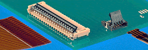
Flexible Circuitry and FPC Connectors
Flexible electronic printed circuitry, commonly called FPC and as mentioned above, has benefited from the development of new materials such as Teflon, polyesters, polyimide, LCPs, and others. During the next decade, FPC will begin to overlap with printed and plastic electronics developments, including new materials, processes, and applications. These new developments will include roll-printed electronic circuitry and other printed circuitry, such as thin-film photovoltaics, RFID tags, and other new technologies, some of which will require interconnect technology.
FPC has followed decades-long evolution to modern circuit applications: materials, processing, and assembly, including laser drilling, to achieve very fine pitch multilayer circuits. Primary drivers for current applications are thin and light mobile electronics. FPC can be shaped, is flexible, and enables thin dynamically active circuits, or thin, flat, and flexible cables, which are a fraction of the thickness of wire-harness alternatives.
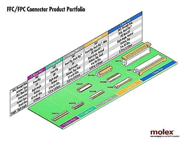
Flex cables and flexible printed circuitry, though similar and often overlapping in application, are hierarchical technologies. Where Flex cables are common arrangements of conductors, pigtails, and connectors for passive point-to-point interconnect applications, FPCs are design-specific flexible printed circuits, often populated with passive and active components. This FPCA has evolved to a leading-edge application, with microvias, flex-rigid capabilities, flip chip, and electronic component assembly. To date, connector technology has kept pace with FPC circuit technology, but during the next decade there may be a dichotomy or compromise between connector size and future micro-miniature FPC geometric capabilities. The table below projects FPC connector and circuit roadmaps, including a current roadmap by Molex, Inc.
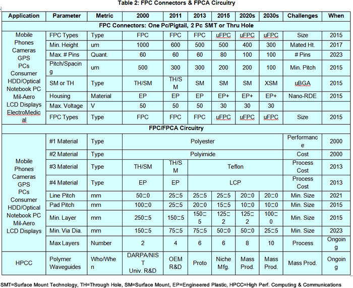
Illustration – Molex FPC Connector Roadmap
- Electric Vehicles Move into the Mainstream with New EV Battery Technologies - September 7, 2021
- The Dynamic Server Market Reflects Ongoing Innovation in Computing - June 1, 2021
- The Electronics Industry Starts to Ease Out of China - November 3, 2020

