The Trouble with Solder: Warpage
The shift from tin lead to lead-free solder has created an unintended consequence that has experts exploring multiple avenues for solutions.
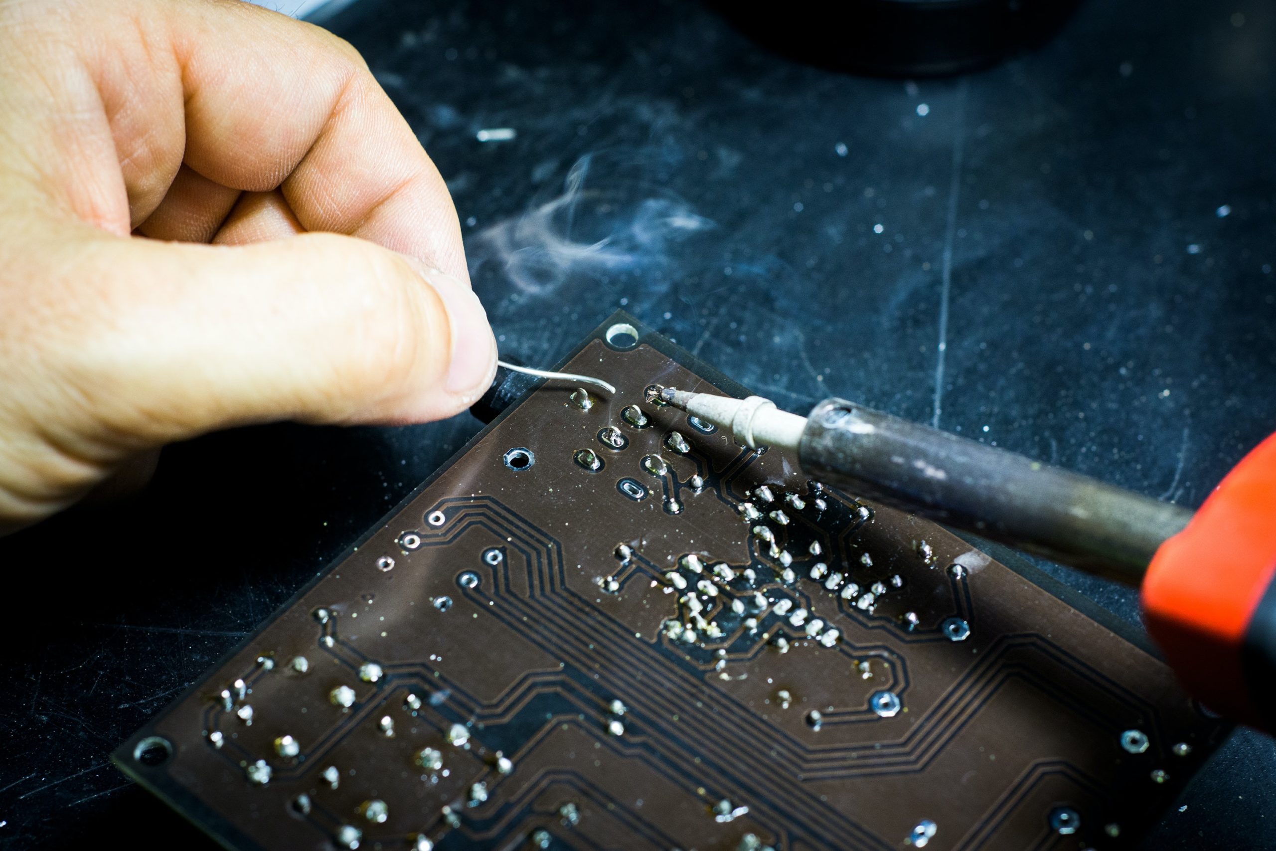
Soldering is the process used to secure connections on a printed circuit board using metal alloys and heat. The two most common types of soldering are reflow and wave. Traditionally, solder was made from a tin lead alloy that is easy to work with and produces excellent results. The shift to lead-free solder necessitates much higher temperatures and increases the chance that parts will warp. Some parts can shrink in height or even no longer be square, which means they may not mate with their cable mate. In an industry where flatness is critical, this is a significant problem.
Reflow vs Wave
Reflow soldering is used for surface-mount technology (SMT), printed circuit boards with the electrical components mounted on the surface. “With surface mount, everything can be made smaller and more components can be put on the real estate of the board with the least amount of space between the components and the board,” explained John Thompson, senior engineering manager, PCBA, BGA, and packaging technologies at Amphenol Communications Solutions. Surface-mount parts are typically used in telecommunications and digital components.
Reflow soldering (also called surface mount soldering) begins with printing a stainless-steel stencil and laser-cutting the area for the circuit. The thickness of the stencil is tightly controlled. Next, solder, an extremely fine powder, is mixed with a flux paste, the cleaning agent used in the soldering process to remove any contaminants or oxides on the metal surfaces. The solder paste is evenly applied to the PCB after the components are temporarily placed on the board, which is typically done with pick and place equipment. It is then heated in an oven for a precise time and temperature during the soldering process.
Wave soldering is for PCBs that use through-hole technology, in which the terminals go through the board, rather than sit on top. Wave soldering is used for power supplies, which generate a lot of current. In this process, the PCB is run over a flux sprayer. At this stage no metal is sprayed, just liquid flux. The board goes over the sprayer and continues up the belt to a molten solder wave bath. The molten solder is pumped from a 400- to 500-pound vat up through a nozzle to create a wave that breaks both forward and backwards, explained Thompson. The wave hits the board as it enters the wave and rolls off as the board exits the wave, creating a rolling action. It wets (adheres) to all the metal surfaces on the bottom of the board.
“Reflow soldering is more of a science. I know if I have my oven set and I can get my temperatures to ABC, my result is going to be XYZ every time. With wave soldering, I can run it the exact same way and if the relative humidity or temperature changes, everything goes out the window. It’s more of an art. You’re fine-tuning it as you go,” said Thompson.
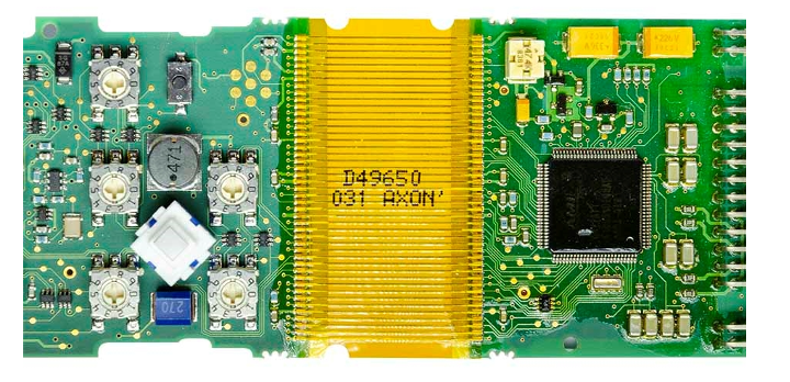
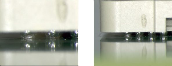
Axon’ Cable’s flat flexible cable (FFC) connected to two PCBs with reflow solder
Pin and Paste
Pin and paste is a version of reflow soldering used for through-hole PCBs. Solder is printed over and through the holes on the board. The through-hole components are inserted through the solder and the boards are run through a heated reflow profile, similar to the process for a surface mount part. “So instead of having two lines where you have a reflow process and then you have a wave soldering process, you now can run your surface mount and through-hole parts through one process,” Thompson explained. “The shortcoming of this, however, is that not all the through-hole parts are able to handle the heat of a reflow. A reflow oven will get from 235°C to 260°C inside the chamber. With a wave solder machine, only the terminal sticking to the bottom of the board is going to get that hot; the components sitting on top of the board stay closer to the ambient temperature of the room.”
Lead-Free Solder and Increased Warpage
“Tin lead, as far as the solder goes, is perfect in every way, except for the fact that it has lead in it. It’s thermally stable, has better creep properties, and its ability to withstand drop shock is very strong,” said Thompson. “The switch to lead-free solder is driving a lot of the change in soldering. It has pushed connector manufacturers to explore different housing materials like LCPs (liquid crystal polymer), which is a resin versus a high-temperature nylon. They tend to handle the temperatures better and are not as hydroscopic, meaning they don’t absorb moisture as fast. And you can mold finer features in them. So as the parts get smaller and finer, you can get more intricate with the molding of the housing.”
The biggest difference between tin lead and lead-free solder is the temperature required to melt them. Ideally, the solder melts and solidifies at a single temperature that is lower than the melting points of the individual components. Tin lead alloy goes from a solid metal to a liquid at 183°C. A typical lead-free alloy, like the industry standard SAC305 — 96.5% tin, 3% silver, and 0.5% copper — melts between 217°C and 221°C and forms a band in the middle of that range. The solder melts up and over the band, making the solder joints less reliable.
With BGA (ball grid array) and other grid array connectors, which are larger connectors, there is a constant fight for flatness, said Thompson. “A three-inch-square array may have 5,000 solder points on the bottom, so the flatness of that part is very important because it must be touching across that PCB. What happens to the flatness of the part going through a heating cycle? If you have a connector that’s going through reflow, it starts to lift. And as the temperature starts to come down and the connector starts to come back down to the board, the solder that’s on the bottom of the connector and the solder on the board may solidify or partially solidify before they come back together, so they don’t coalesce. That’s the main defect that we’re finding in the industry because of warpage. It’s called ‘head in pillow’ because it looks like a pillow after someone has had their head on it.”
Examples of the “head in pillow” effect. Images courtesy of Amphenol Communications Solutions.
What is Being Done to Correct This Issue
Experts are working on the warpage problem from many different angles. Thompson is a member of the International Electronics Manufacturing Initiative (iNEMI) developing a software tool to predict the warpage of connectors as they go through the soldering process. He also works with some of the larger OEMs developing new alloys that have a lower melting temperature to help reduce the amount of warpage. A new bismuth-based alloy that melts at approximately 150°C, about 100 degrees cooler than other lead-free alternatives, shows promise but has poor drop-shock resistance. It is getting attention from the big computer manufacturers who are experimenting with adding proprietary materials to make it less drop-shock sensitive.
“The elevated temperatures cause a lot of problems for us. We’re doing a lot with resins, with predictive software, with changing alloys. We’re also looking at different types of boards, at different types of designs, and at different molding technology. It’s pushing all the envelopes, but it’s all being driven by flatness, trying to keep parts flatter,” said Thompson.
To learn more about the companies mentioned in this article, visit the Preferred Supplier pages for Amphenol Communications Solutions and Axon’ Cable.
Like this article? Check out our other Manufacturing, Contacts and Innovation articles, our Materials Market Page, and our 2022 and 2021 Article Archives.
Subscribe to our weekly e-newsletters, follow us on LinkedIn, Twitter, and Facebook, and check out our eBook archives for more expert-informed connectivity content.
- Extreme Temperature Innovations for Aerospace and Defense - July 21, 2026
- Connectors for Soldier Systems Product Roundup - July 21, 2026
- July 2026 Connector Industry News - July 21, 2026