Miniaturized Smart Devices Pose Larger Design Challenges for Interconnects
Smaller, more powerful, and connected new device designs call for more antennas, PCB connectors, and other components. The challenge is to make them all fit. Strategic antenna selection and positioning is the first step in preserving performance and reliability.

Electronic devices are increasingly utilizing one or more wireless technologies to become connected to the Internet of Things (IoT). Smart IoT devices like mobile phones, watches, and medical devices are just a few of many technologies that have become more powerful through interconnected capabilities. However, the integration of multiple wireless technologies into miniaturized IoT devices presents unique design challenges. Many of these devices are also portable, wearable, or operate in harsh environments and must deliver long battery life and high performance. Approaching the design phase with a holistic view of the impact of all components—including antennas and PCB connectors—is a critical step to avoiding unanticipated performance issues that can result in late-stage design changes, higher expense, and delayed time to market.
In smart devices, antennas are an important connection. As device sizes have scaled down, so have antennas, but strategic device design is still needed. Ground plane dimensions, distance to nearby components, antenna position, PCB layout, and component selection all impact device performance. Cutting-edge technologies, such as laser direct structuring (LDS) and metamaterial antenna technology, are among the innovative solutions available to minimize the space needed for antennas in smart devices.
Ground plane size and antenna selection
The size of the ground plane is often dictated by the size of the device. For monopole or monopole-based antennas, ground plane size is critical for good antenna performance. It should be at least λ/4 in size, where λ is the wavelength of the lowest frequency band of the monopole antenna. For lower cellular frequency bands (698-960 MHz), the λ/4 would be around 107 mm. A ground plane of this size would not be suitable and possible for most IoT devices due to their small form factor. Therefore, a design consideration could be made to avoid monopole-based antennas, which are dependent on the ground plane for good performance. Other antennas, such as dipole, could be used to overcome the ground plane size problem. Sometimes it is possible to extend the ground plane vertically if the height of the device allows. This technique makes it possible to have a large enough ground plane for monopole antennas for higher frequency bands, such as 2.4 GHz or 5 GHz.
Distance between components
Most antenna data sheets recommend a clear-out zone for the antenna to deliver optimum performance, as nearby components can have an impact on antenna performance. Some components, such as the battery, display, and charging coil, could detune the antenna. Surface mount device (SMD) components located close to the antenna could detune and decrease the antenna’s efficiency. A custom antenna design that mitigates the impact of nearby components may be necessary to achieve optimum antenna performance in some environments.
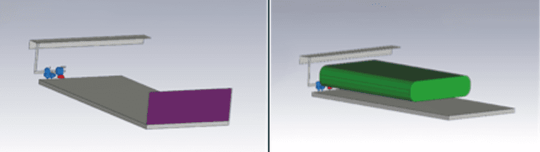
Extended vertical ground plane (left). Positioning the battery a few millimeters away from the antenna requires a custom antenna to mitigate the impact (right).
Antenna position
In small smart IoT devices, it is difficult to respect the clear-out zone requirements for the antenna. One solution could be to choose an antenna with a cable of a certain length to be mounted on the device housing away from the PCB. Another option would be to print the antenna on the inner or outer side of the housing, creating additional free space around the antenna and decreasing the impact from other components. It is very important to make sure that the housing material does not affect the printed antenna parameters and is not lossy on the desired frequency bands of operation.
PCB layout and component selection
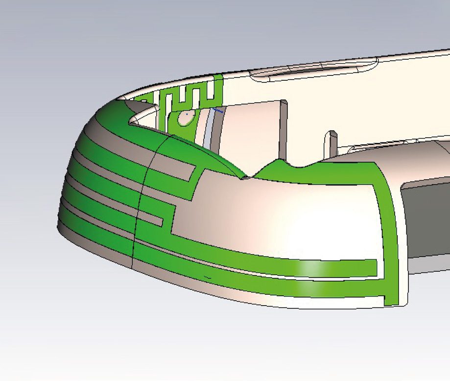
Antenna modeled on a device plastic housing using LDS
The choice of components mounted on the PCB is also very important in miniaturization. By selecting smaller components and connectors, it is possible to create more free space for the antenna and greater physical and electrical distance from other components. This helps in providing higher isolation and lower mutual coupling. It is also critical to have a clean radio frequency (RF) ground plane without any signal routing on the antenna ground plane. High-speed data lines should be kept away from the RF lines.
Laser Direct Structuring (LDS)
LDS is a state-of-the-art technology used to create molded interconnect devices (MIDs) and can save valuable space in your application by integrating high frequency, mechanical, and electrical functionality into one component. Laser structuring enables 3D design/routing capability, versus the limiting 2D capability on a PCB or other common substrates. LDS also allows for improved antenna performance because antennas can be placed in the design where they have more room for better bandwidth and efficiency. The use of LDS technology is not limited to antennas, but can also be used for electromechanical, shielding, and other components across an array of applications.
Metamaterial Antenna Technology
MetaSpan antennas from TE Connectivity use metamaterial antenna technology and are intrinsically designed with capacitive coupling and inductive loading. The benefits of this technology include enhanced low-band bandwidth and efficiency, reduced antenna size, intrinsic matching, improved stability compared to body loading, and confined currents on or near the structure to prevent coupling with adjacent RF components or other antennas.
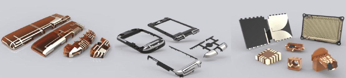
Examples of LTE, GNSS and Bluetooth antennas using MetaSpan antenna and LDS technologies.
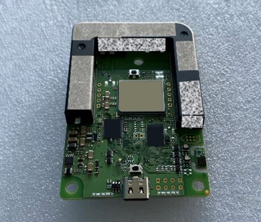
MetaSpan on the board
Another important consideration for the design of miniaturized IoT applications is proper connector selection. Read this article in its entirety for a deeper dive into antenna design, the many connector types that serve IoT designs, and how to best implement them in your design by downloading TE Connectivity’s new white paper.
Additionally, please attend the webinar Miniaturization Considerations for Smart Internet of Things (Iot) Devices on August 25, 2022, at 10 a.m. EST.
Visit TE Product Solutions to learn more about components for the Internet of Things.
By Irfan Yousaf, TE Antenna Solutions Expert and David Currie, TE Product Manager at TE Connectivity.
Like this article? Check out our other IoT and antennas articles, our Datacom Market Page, and our 2022 Article Archive.
Subscribe to our weekly e-newsletters, follow us on LinkedIn, Twitter, and Facebook, and check out our eBook archives for more applicable, expert-informed connectivity content.
- Bringing Modularity to Multi‑Board Systems - June 30, 2026
- Engineering’s Future is AI-Inspired, Human-Led - June 23, 2026
- How High-Reliability Connectors Meet the Demands of Satellite Engineering - June 23, 2026