CCSI: Connector Crime Scene Investigation
Next up in our “Connector Basics” series, APEX Electrical Interconnection Consultants offers advice on when and why you need someone with failure analysis expertise.
 Something is not working out in the connector manufacturing process or, worse yet, a connector fails in the field – in either case, the failure should land on the workbench of an investigator. It could be either an internal investigator employed by the manufacturer or an independent lab, an independent consultant, or a consulting group. The second option is especially common for smaller companies that tend not to have their own internal resources to conduct an adequate investigation. Larger corporations might have their own investigation units, staffed by engineers and technicians, who have sufficient on-site equipment. This, however, is becoming increasingly less common. In their drive to lower costs, even the large corporations are cutting their failure-investigation departments and outsourcing the investigative work to independent entities.
The shift to the outside investigators, while lowering the costs of manufacturing, creates its own problems, for the companies in particular and the industry in general. Companies might be concerned with proprietary information leaks. As for the industry, the industrial capacity might be negatively affected, since the experts capable of conducting a proper investigation are no longer employed by the corporations. The former issue is usually adequately resolved by signing a non-disclosure agreement. The latter problem (comprehensively described in a previous article in this series) is currently resolved, to a large extent, by the experts formerly employed by corporations, who form their own consulting companies and laboratories.
The current globalization trends make the decrease in failure analysis experts even more severe, as the amount of lower-quality products is increasing. Additionally, the trend toward miniaturization, shorter time-to-market, shorter product lifespan, and the demand for higher quality has resulted in an increasing need for a larger pool of qualified investigators.
Perhaps one bright spot in this rather gloomy landscape is the increasingly capable technologies that could be used to rapidly and cost-effectively analyze the failures. Let’s take a look at some of these technologies. First, we’ll examine the course of action in failure investigations.
Initial Inspection/Optical Microscopy
As the failure lands on the investigator’s desk, a simple examination by the expert might be sufficient to resolve the problem. A magnifier or an inexpensive optical microscope could be used in this investigation. Any problem caused by corrosion, for example, would be easily recognized and characterized by an expert in the majority of cases. The same goes for most types of contamination. For connectors in particular, fretting corrosion often can cause failure and would be recognized and characterized. Of course, initial observation is limited to the surface of the subject of investigation, unless a fracture is part of the failure. In case of fracture, its surface also can be examined as a part of the initial investigation.
A good example here would be visual quality of a crimp. If a crimp does not appear quite right, it could be easily tested by a pull test. Generally, if the pull-out force is less than 70% of the tensile yield stress of the wire, it would require further investigation to determine the root cause.
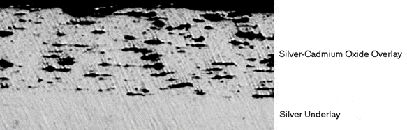
Below is an example of a manufacturing problem. In this case, optical microscopy was used together with cross-sectioning to identify the problem. Switches using a silver-cadmium oxide overlay on a silver underlay failed incoming engineering and reliability tests after very few test cycles. Failures were found where the switch contacts were welded together. Contact welding during accelerated testing resulted from a pure silver layer on the surface of the contacts rather than silver-cadmium oxide as desired. The silver cadmium oxide overlay was fabricated in a two-layer flat ribbon form and improperly inverted when bonded to the body of the rivet. The overlays were clearly visible and identifiable in cross-sections. Here is a typical example of silver-cadmium oxide overlay as it appears in a cross-section.
In most cases, simple observation is not enough to conclusively resolve the problem and a wide array of analytical tools are available. Below are some examples.
Electron Microscopy
The scanning electron microscope (SEM) long ago transformed from an exotic university/laboratory research tool to a common workhorse of the failure investigation trade. Not only can it provide very high magnifications compared to the optical microscope, but it is also capable of rapid elemental analysis, qualitative or semi-quantitative. Of course, like any other microscope, it can observe and analyze only the surface of the sample; however, it can be combined with conventional cross-sectioning to carry out analysis of subsurface areas.
The SEM can be used in three modes:
- Secondary electrons mode (SE) is the most common. The image is produced by the secondary electrons generated by the scanning electron beam. These electrons are emitted from the surface and produce the image of the surface topography.
- Backscatter electrons mode (BSE) is less common. In this mode, a special BSE detector picks up the original beam electrons that bounce back after hitting the specimen. The amount of bounce depends on the atomic number of the material – heavier elements produce more bounce and appear brighter in the image. Therefore, BSE mode can offer information on the material composition that could be helpful in the analysis.
- Energy dispersive spectra (EDS) or energy dispersive analysis of x-rays (EDAX) produces elemental composition of the scanned surface area. The scanning electron beam generates x-rays that are emitted from the top layer of the surface. Each element has a characteristic x-ray spectrum, so this technique gives us the elemental composition of the surface layer. Ultimately, the surface can be mapped for the elements present at the surface. A major disadvantage of this mode is the slow speed; it takes time to accumulate enough x-ray to identify the spectra in a statistically significant manner. This is especially true for the element mapping, since in this case spectra are acquired at each point of the scan, pixel by pixel.
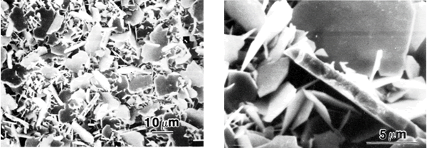
Below is an example of SEM analysis that deals with intermetallic compound growth in a plated tin or tin-lead finish. Nickel underplating is generally very efficient to preserve solderability; however, components stored for extended time at elevated temperatures (sea transportation or warehouses with no climate control) do not solder well. The reason for loss of solderability become evident when tin is chemically stripped from the plating and samples are examined under SEM. The examination revealed a previously unknown type of tin-nickel intermetallic compound growth. Here are typical samples of this growth, as imaged by the secondary electrons.
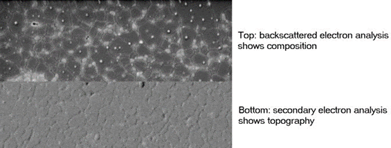
Below is a sample image comparing a secondary electron image with a backscatter electron image. This particular sample was a beryllium-zirconium-aluminum alloy.
X-Ray Radiography
The analytical techniques described so far apply to the study of surfaces. The only way to obtain information from the bulk of the samples is to cross-section it as in the first example or chemically strip a selected part of it as in the second one. Cross-sectioning has its advantages, such as ability to obtain the elemental composition, but there are major drawbacks. It is slow, it requires experienced technicians, and the sample is destroyed in the process. Most importantly, it gives us information on just one plane. Of course, it is possible to extend the number of planes investigated by grinding/polishing down the sample, but it could be too time-consuming and expensive for practical use. Selective chemical stripping is faster, but only applicable in specific cases, and it also has its own disadvantages.
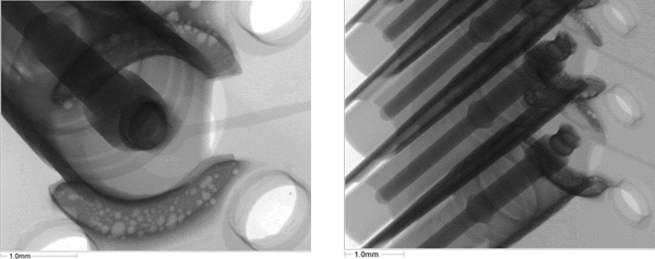
Fortunately, there is a way to look below the surface and inside the object by using penetrating radiation, most commonly x-rays. Industrial radiography has been used for a long time as a non-destructive inspection technique. Some fairly recent developments in radiography greatly increase its potential applications in the case of connectors. Microfocus technology allows a large magnification of x-ray images, so relatively small components can be examined in detail.
Below are typical images produced by microfocus equipment. The sample examined is a PC board with soldered components. It clearly shows voids in the solder fillets.
Combining high-resolution x-ray imaging with computing power allows three-dimensional reconstruction of the rather small objects at high resolution. The technique is called x-ray microtomography or micro-CT. Micro-CT allows us to cut virtual sections or even scan the computer-generated 3D images of the samples non-destructively. No preparation, coating, or vacuum treatment is needed. Micro-tomography is available in a range of easy-to-use desktop instruments, which generate 3D images of the sample’s morphology and internal microstructure with resolution down to the sub-micron level. The only drawback compared to the regular cross-sectioning is that we do not get the information on the internal elemental composition, although denser materials will appear darker. However, if the regular cross-sectioning must eventually be done to obtain the chemical composition, micro-CT will remove any guesswork of where the cross-section must be located to produce the desired information. One can find many examples of the use of micro-CT in electronics manufacturing and failure analysis online.
The techniques listed above are not an exhaustive list of available tools, but some are most likely to be employed in determining connector problems. In any case, if and when a problem arises, and the internal recourses are not sufficient to solve it, turning to an experienced investigator and these available tools would most likely lead to resolution.
[hr]
Author Joseph Haimovich, Ph.D., is a senior consultant at APEX Electrical Interconnection Consultants. He has more than 28 years experience in the connector industry and specializes in the metallurgy of base materials, contact coatings, solders, and finishes, particularly tin and tin alloys, as well as lead-free finishes. Haimovich’s experience spans intermetallic compound formation and growth and diffusion and corrosion in solders and contact coatings, including their effects on solderability and contact properties, tin whisker growth, and tin pest prevention.