Over-the-Board Cable Solutions Raise the Speed Limits on Board Designs
As bandwidth grows and speeds continue to accelerate, conventional PCB solutions are reaching their limits. Over-the-board cable solutions alleviate heat and signal integrity concerns while allowing systems to reach ever higher performance levels.
By Jim David and Vishal Chandrasekar, Amphenol Communications Solutions
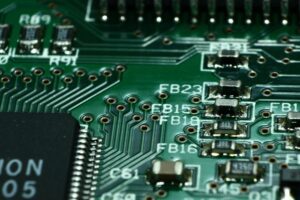
In today’s data driven world, manufacturers of switch, server, and router hardware are continually challenged by internet service and network providers — and by their clients in financial, academic, and research institutions — to deliver hardware that is higher capacity, faster, and delivers greater overall bandwidth. Chip manufacturers are filling this need with 56G and 112G chip sets. However, these signaling speeds have highlighted the performance and application limitations of conventional PCB solutions (high performance board laminates, signal re-timers, etc.) and have forced hardware architects to look for new ways to deliver these higher speeds in their designs.
A solution to these challenges is over-the-board cable technologies. These solutions not only satisfy electrical and mechanical system requirements, but also meet the increasingly challenging signal integrity (SI) and thermal requirements of most high-performance system designs.
Amphenol Communication Solutions’s OverPass™ integrated interconnect system solution addresses stringent system requirements while meeting the SI performance of 56G, 112G, and 224G speeds.
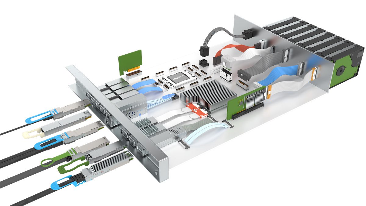
These products create a direct, high-performance interconnect from the connector at the external port of the system to a connection point near the chip, or one mounted directly on the chip package itself. This approach creates an “overpass” for the signals – bypassing the PCB and significantly lowering overall signal loss. This design strategy also eliminates the need for costly low loss, exotic PCB laminates and power-hungry, heat generating signal re-timers.
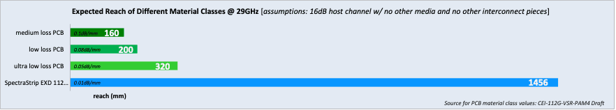
The chart below shows the relative loss for different PCB laminates – from conventional to high performance – and compares them to a typical over-the-board bulk cable. The cable-based approach delivers a range that is four or five times larger relative to even the high-cost, ultralow-loss PCB materials.
Over-the-board cable solutions consist of three components: IO interfaces (external IO, backplane), high-performance differential pair bulk cable, and high-density, low-profile IO connector systems for near chip or on-package mounting. The external IOs are usually industry-standard connector interfaces like SFP, QSFP, QSFP DD, and OSFP, and are available in single port, ganged, or stacked cage configurations. These connectors can be customized to include heat sinks and light pipes as needed. The high-speed differential pair cables can support 56G, 112G, and anticipated 224G signaling speeds and can be customized to any length.
The near chip/on package solutions for 112G/224G applications include DensiLink and micro-LinkOVER. Differential pair wires are terminated very close to the contact beam, resulting in highly efficient signal transfer between the cable and the contact pad on the PCB or chip package. Both boast impressive differential pair (DP) density – micro-LinkOVER with a density of 3.1 DP / cm2 and DensiLink with densities of 9.3 and 10.7 DP / cm2, depending on configuration. This high density, along with the ability to mount these connectors in an array matrix, enables over 1,000 cable interconnections around the periphery of chips. The low height profile of these connectors enables assembly close to switch chips and under heatsinks, further reducing overall trace loss.
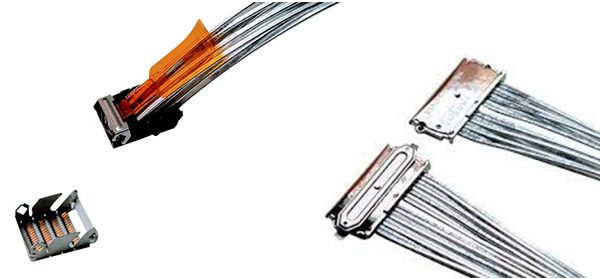
Amphenol’s DensiLink®IO and micro-LinkOVER™ cable products.
Attention must be paid to ensure these cabled solutions are properly applied and assembled into the hardware systems to meet the stringent high speed signaling and transmission requirements. Early and frequent discussions between suppliers and customers, particularly during the product definition stage, is critical to ensure all “design for assembly” factors are properly considered.
One example is IO pin mapping and cable routing. Straight cable routing (point to point without crossovers) makes for a straightforward product assembly process but may not meet every customer application. Crossover wiring, particularly with multiple IO cages and multiple near-chip ends, needs to be assembled with careful consideration for the multiple cable lengths and routings involved. Consideration of multiple Rx and Tx IO patterns is not unusual.
Such upfront discussions result in processes that define the order in which the cable ends are assembled and terminated in the system, assuring proper cable routing and management, and deliver a solution better aligned with end customer expectations and assembly practices versus one done in absence of engineering and design collaboration.
The early involvement of hardware system designers to ensure proper product definition and deployment is essential to the design of a successful over-the-board strategy. Looking to future signaling speeds and applications, and the limitations of conventional PCB materials, while this approach is advantageous at 56G signaling, it will be absolutely necessary to extend the use of copper-based cabling solutions in hardware designs at 112G and 224G signaling.
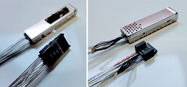
Amphenol’s QSFP DD OverPass™ and OSFP OverPass™ over-the-board solutions.
Learn more about Amphenol’s extensive integrated interconnect solutions, including optical modules, AOCs, passive and active DAC cables, backplane cabling, and other high-speed and power interconnect solutions.
Like this article? Check out our other Wire & Cable and New Technology articles, our Datacom/Telecom Industry articles, and 2022 Article Archives.
Subscribe to our weekly e-newsletters, follow us on LinkedIn, Twitter, and Facebook, and check out our eBook archives for more applicable, expert-informed connectivity content.