New Socket Solution Optimizes Production Testing of QFN-packaged ICs
Advances in semiconductor functionality, density, and chip-level integration are generating new challenges in testing. A test socket solution overcomes the challenges posed by traditional vertical spring probes and cantilever scrubbing contact designs, providing a new level of performance and reliability.
Integrated circuit (IC) designers are increasingly migrating to quad flat no-lead (QFN) packages to meet the needs of applications that have a small outline or low-profile footprint yet still require best-in-class electrical requirements and performance. QFN packages feature direct-attach peripheral pad structures, a large ground block for thermal and electrical performance, and a very thin stack height, making them ideal for many designs, but they also bring some challenges to the Test & Measurement process. To meet these testing challenges, a test socket solution that is robust, reliable, and electrically “clean” is needed.
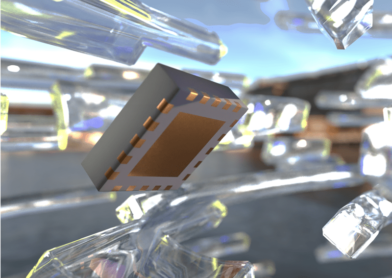
Quad flat no-lead package, or QFN, packs performance into a is a low-profile IC package.
As logic chips become more advanced, we are seeing a corresponding increase in pin counts, power consumption, and BGA package structures. However, for the majority of analog, mixed-signal, power, and RF devices, power and pin count take a back seat to electrical performance and reliability. Fabricated primarily on legacy (>16 nm) process nodes, these devices tend to have small numbers of I/O connections and ganged power connections. Device manufacturers make use of QFN packages to improve electrical performance while reducing the size, weight, and footprint of the equipment.
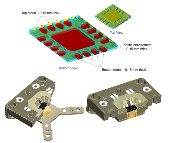
QFN packages use traditional wire bonding and molding encapsulation techniques to protect the silicon die. They also use “near chip scale” pad layouts on the periphery, along with a large “ePad” or “exposed paddle.” With electrical pads fully contained inside the outline of the molded plastic package body, QFN’s eliminate many of the handling and reliability challenges of their QFP and SOIC predecessors. When a QFN is soldered onto a PCB, the connection is as short as possible, and – aside from certain coefficient of thermal expansion (CT) considerations – extremely robust. QFN’s feature a very large ground pad in the center of the rectangular package body, which facilitates not only excellent electrical performance, but greatly improves thermal dissipation. Instead of venting heat generated by the IC upward through the package body, the heat in a QFN ePad can be drawn downward into the PCB to thermal vias, greatly improving stability and performance.

Test & Measurement evaluations of QFN devices ensure robust and reliable performance over hundreds of thousands of insertions while maintaining extremely clean signal paths. In many cases, the device under test (DUT) will have RF requirements exceeding 10 GHz or more, inductance specs that must be carefully managed, and very low contact resistance targets. At the same time, costs must be minimized.
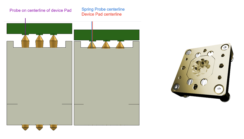
To balance these needs, engineers look for a test socket solution with a short, highly controlled signal path and a robust mechanical structure. One key element of the mechanical structure that warrants special consideration is the wear rate on the surface pad of the PCB load board used to connect the socket to the automated test equipment (ATE). Load board costs routinely exceed $50,000 to $75,000, making it imperative that the socket actuation cause as little damage to the surface pads as possible. If the test socket causes pad damage, the test operations team may need to re-plate the PCB’s surface pads, or, worse, replace the entire PCB.
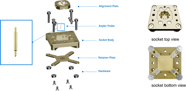
Smiths Interconnect’s Kepler test socket is a proven solution that balances both the electrical targets and the high-volume manufacturing (HVM) requirements for today’s advanced QFN-packaged ICs. Designed for manual, bench, and HVM production testing, this test socket delivers two axes of motion in a single stroke, providing best-in-class electrical length, inductance, and contact resistance for sub-20GHz test applications. The X-Y axis motion of the contact breaks surface oxides with the same impact on PCB load board pads as a vertical spring probe, allowing for hundreds of thousands of cycles with little to zero maintenance. The Kepler is footprint-compatible with existing QFN offset socket solutions and can be implemented in short order for demanding high-volume IC applications.
Smiths Interconnect’s Kepler Test Socket allows for PCB topside components to be placed close to DUT for better signal performance and less signal loss.
As chip updates become faster and more complex, evaluation and qualification processes are evolving to provide higher test reliability in less test time. To realize these goals, a new generation of Test & Measurement components feature optimized design and superior mechanical performance. Today’s test processes are an essential step in the goal to help designers successfully engineer new products and get them to market quickly.
Visit Smiths Interconnect to learn more about test solutions, including test sockets and reliable spring probe technology.
Like this article? Check out our other Test & Measurement articles, our Special Topics Page, and our 2023 and 2022 Article Archives.
Subscribe to our weekly e-newsletters, follow us on LinkedIn, Twitter, and Facebook, and check out our eBook archives for more applicable, expert-informed connectivity content.
