Optimizing PCB Stack-up for High-speed Connectors
Learn how to optimize a printed circuit board (PCB) stack-up with high-speed board-to-board interconnect solutions.
Article Contributed by I-PEX
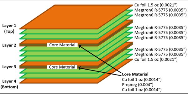
A PCB stack-up defines the cross-sectional structure of a PCB. It defines the arrangement of copper and dielectric layers within the PCB. Figure 1 is an example of a typical 4-layer board – all copper and dielectric layers are identified with their thickness. The stack-up definition plays a critical role in achieving the desired signal integrity, thermal performance, and manufacturability. The following should be considered before defining a PCB stack-up:
- Signal Integrity / Impedance Control – High-speed signal traces are placed adjacent to a solid reference plane (ground or power) to establish a transmission line with controlled characteristic impedance. The characteristic impedance depends on the trace width, copper thickness, and the dielectric characteristics of the dielectric material.
- Electromagnetic Compatibility (EMC) – Alternating signal layers with ground or power planes helps confine electromagnetic fields within the PCB, thereby reducing electromagnetic emissions and minimizing interference.
- Thermal Management – A well-designed PCB stack-up facilitates effective heat dissipation from high-power components to prevent localized hot spots and thermal damage.
- Manufacturability and Cost: The PCB stack-up should be designed within the manufacturer’s fabrication capabilities. Key considerations include material selection, layer count, trace dimensions, and via structures. Manufacturing tolerances should also be considered to ensure consistent quality and reliable performance.
When a high-speed connector is mounted on a PCB, the stack-up may require further optimization to achieve the connector’s maximum signal integrity. Although it is not necessary for every connector, many high-speed connectors, including the I-PEX NOVASTACK series, rely on the capacitive coupling between the signal pins and the PCB ground plane to achieve the intended characteristic impedance. In typical PCB stack-ups, this optimization is often accomplished by removing copper from the top layer directly beneath the connector – see Figure 2 and Figure 3. This allows designers to optimize the separation between the connector pins and the reference ground plane by selecting an appropriate PCB stack-up.
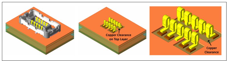
Figure 2 Ground clearance on top layer (Example: NOVASTACK35-HDN Plug)
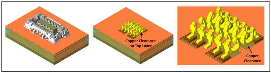
Figure 3 Ground clearance on top layer (Example: NOVASTACK 35-HDN Receptacle)
The cross-section of a mated NOVASTACK 35-HDN connector on a 4-layer PCB is shown in Figure 4. For clarity, only the connector pins are shown to highlight the copper clearance on the top layer. The capacitance between the connector pins and the reference ground plane is represented as CPIN2REF. This capacitance can be controlled by adjusting the distance between the top layer and the reference ground plane.
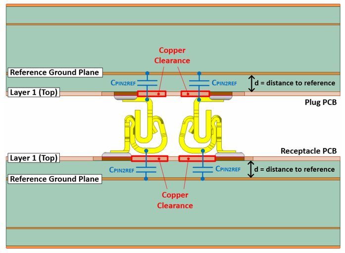
Figure 4 Cross-section of PCB and mated NOVASTACK 35-HDN (only pins shown)
In PCB stack-ups with more than four copper layers, the copper clearance may be required on multiple layers to ensure the optimal separation between the connector pins and the reference ground plane. This concept is illustrated in Figure 5. In this example, copper is removed from Layer 1 (Top), Layer 2, and Layer 3 to achieve the desired capacitance between the connector pins and the reference ground plane on Layer 4.
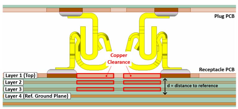
Figure 5 Cross-section of multi-layer PCB and NOVASTACK 35-HDN (only pins shown)
The following case study demonstrates how a simulation tool can be used to determine the optimal distance between the top layer (Layer 1) and the reference ground plane – refer to Figure 4. This simulation example uses the NOVASTACK 35-HDN connector in a differential configuration. The corresponding port assignment used in the simulations is illustrated in Figure 6.
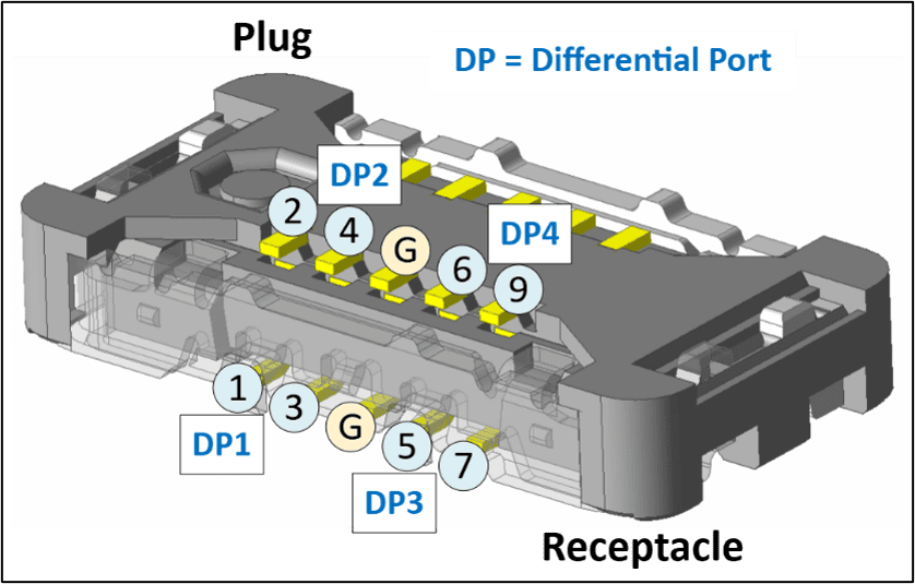
Figure 6 Port assignment used in simulation
The CST studio simulation varies the distance between the top layer (Layer 1) and the reference ground plane, denoted as d in Figure 4, from 0.05 mm to 0.35 mm in 0.05 mm increments. The simulations are performed for the reference impedance of 85 ΩDIFF and 100 ΩDIFF to determine the optimal d for each impedance.
The simulation results for the reference impedance of 85 ΩDIFF and 100 ΩDIFF are shown in Figure 7 – Figure 10 and Figure 11 – Figure 14, respectively.
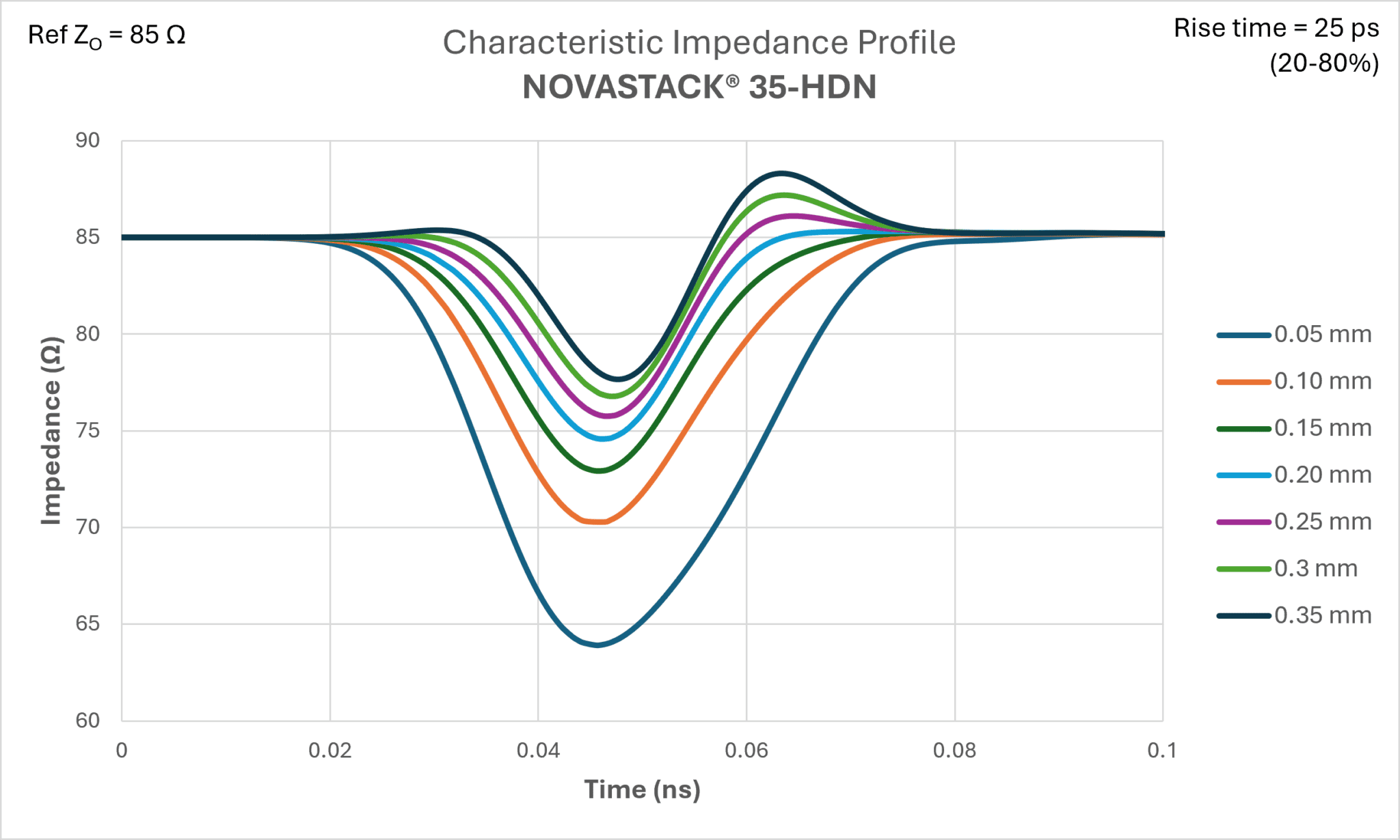
Figure 7 Impedance profile of NOVASTACK 35-HDN (Reference ZO = 85 ΩDIFF)
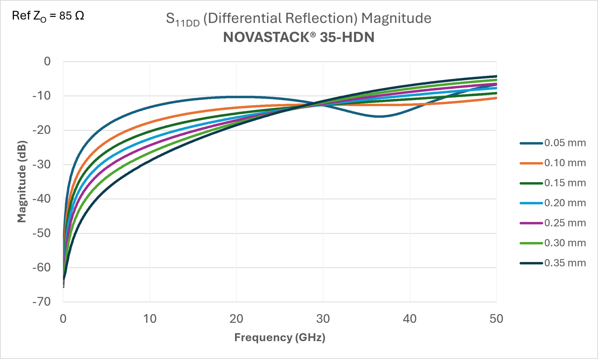
Figure 8 Differential reflection (S11DD) of NOVASTACK 35-HDN (Reference ZO = 85 ΩDIFF)
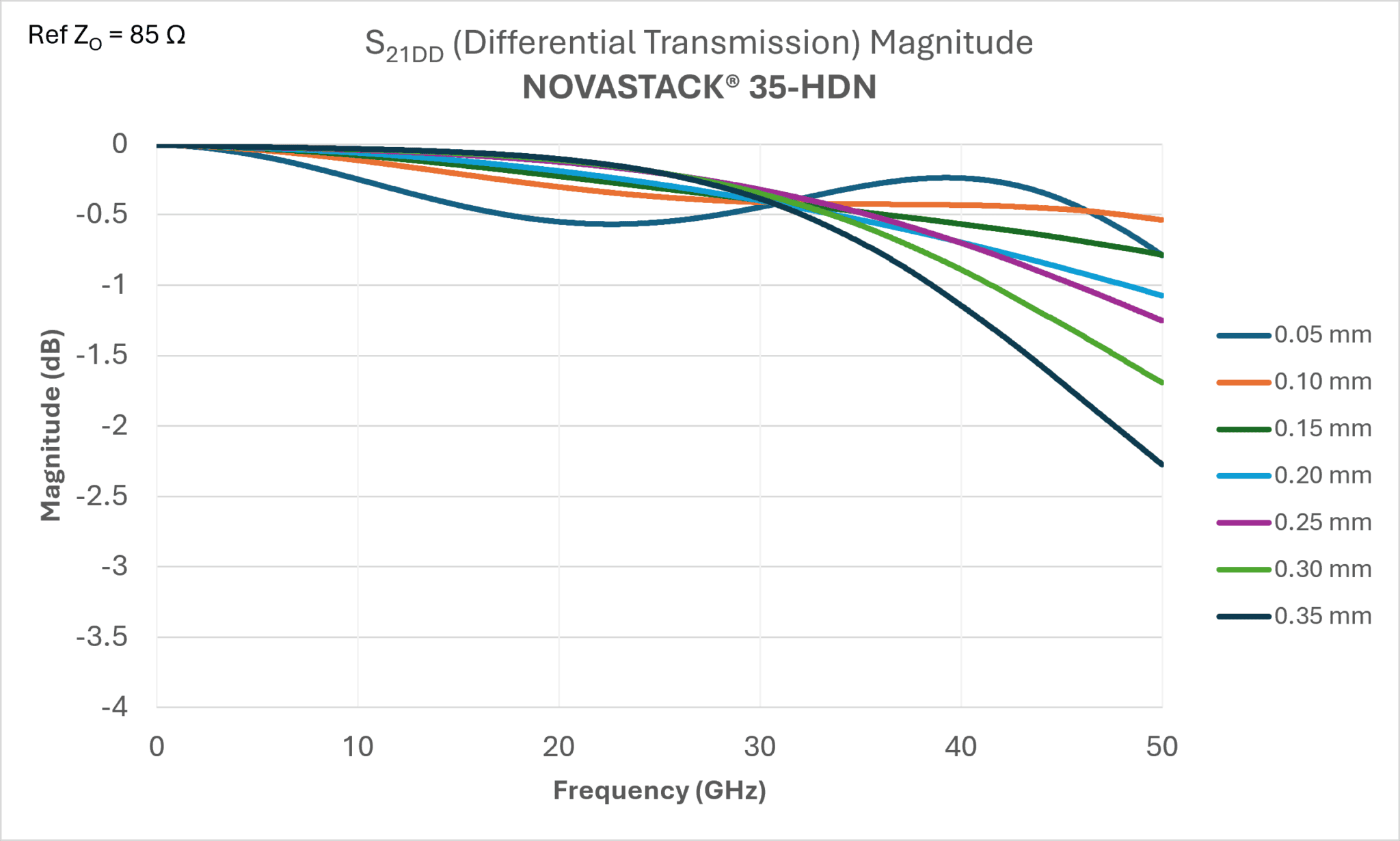
Figure 9 Differential transmission (S21DD) of NOVASTACK 35-HDN (Reference ZO = 85 ΩDIFF)
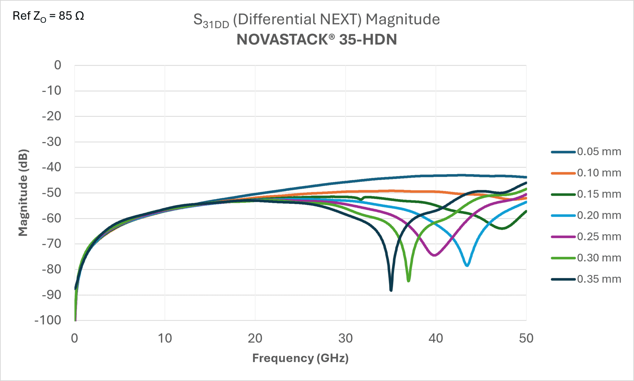
Figure 10 Differential NEXT (S31DD) of NOVASTACK 35-HDN (Reference ZO = 85 ΩDIFF))
Visit I-PEX to see more solutions for high-speed design.
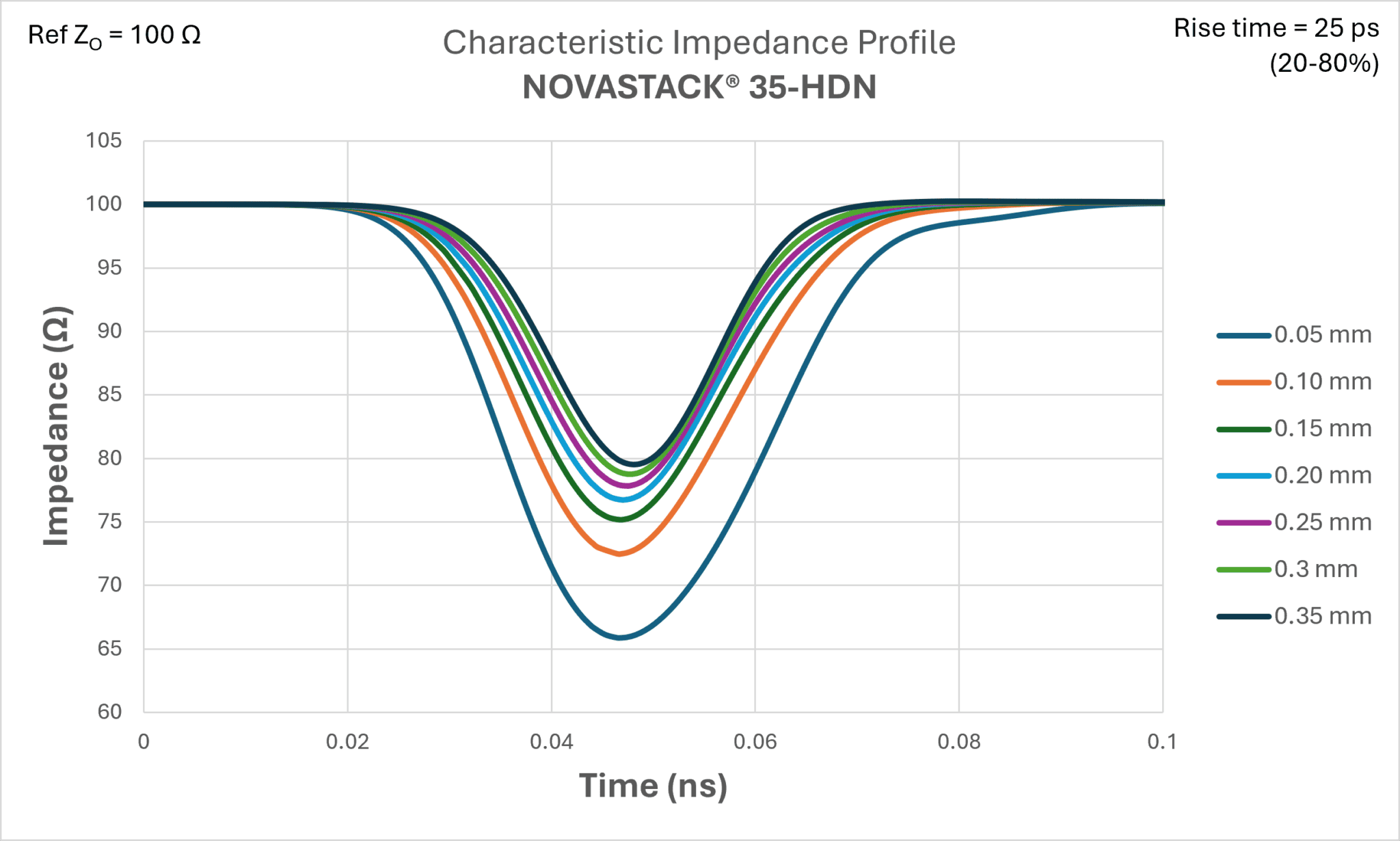
Figure 11 Impedance profile of NOVASTACK 35-HDN (Reference ZO = 100 ΩDIFF)
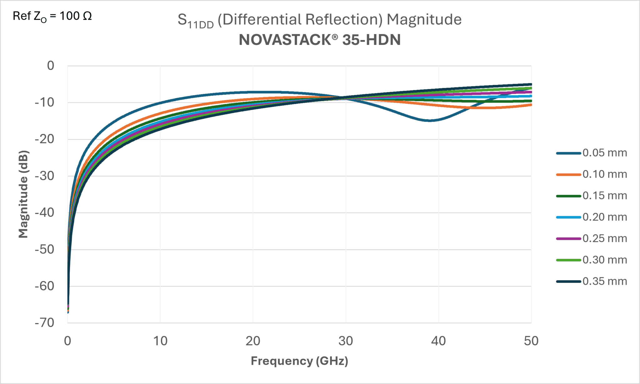
Figure 12 Differential reflection (S11DD) of NOVASTACK 35-HDN (Reference ZO = 100 ΩDIFF)
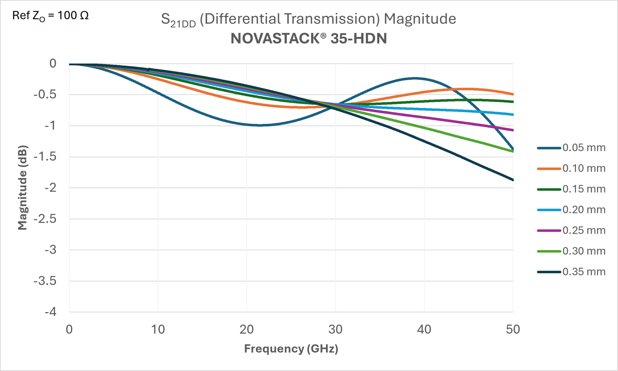
Figure 13 Differential transmission (S21DD) of NOVASTACK 35-HDN (Reference ZO = 100 ΩDIFF)
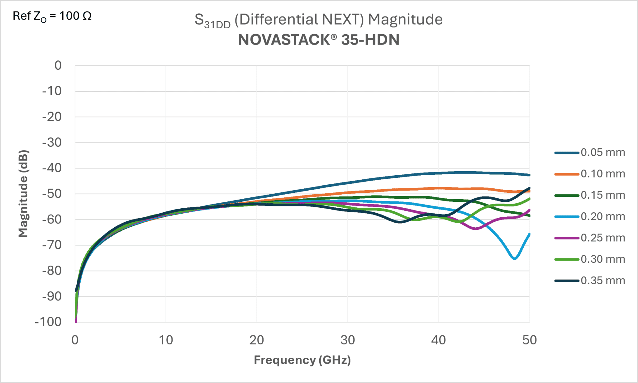
Figure 14 Differential NEXT (S31DD) of NOVASTACK 35-HDN (Reference ZO = 100 ΩDIFF)
The following observations can be made about the NOVASTACK 35-HDN connector:
- The characteristic impedance of NOVASTACK 35-HDN increases as d increases (CPIN2REF decreases).
- Below 29 GHz, the differential reflection (S11DD) improves as d
- Above 29 GHz, the differential reflection (S11DD) degrades as d
- The near-end crosstalk is suppressed below 40 dB in a differential configuration.
- The characteristic impedance of NOVASTACK 35-HDN is closer to 85 ΩDIFF
The distance between the connector pins and the reference ground plane can be optimized based on the application requirements:
- For transmission bandwidths below 29 GHz, d should be maximized to minimize S11DD while maintaining acceptable S31DD.
- For transmission bandwidths above 29 GHz, reducing d improves S11DD at higher frequencies; however, this improvement comes at the expense of degraded S11DD at lower frequencies. Therefore, d should be carefully selected to accommodate all frequencies for S11DD.
The simulation results demonstrate that the spacing between the connector pins and the reference ground plane is a key design parameter affecting the electrical performance of the NOVASTACK 35-HDN connector. While larger values of d are advantageous for lower-frequency applications, smaller values improve differential reflection (S11DD) at higher frequencies. Therefore, the optimal value of d depends on the transmission bandwidth and design objectives. Based on the simulation results, I-PEX selected d = 0.20 mm for the NOVASTACK 35-HDN test board because it provides the best overall S11DD performance across the full frequency range.
I-PEX specializes in designing and manufacturing high-speed interconnect solutions with customizable pin counts and cable configurations. Its products support a wide range of high-speed interfaces including MIPI (D-PHY and C-PHY), PCIe, USB, eDP, and Thunderbolt. The NOVASTACK 35-HDN connector is just one example of I-PEX’s high-performance interconnect solutions. The diverse I-PEX product portfolio delivers exceptional signal integrity while offering the mechanical reliability and design flexibility needed for a wide range of applications. For more information about products and solutions, contact I-PEX.
Like this article? Check out our other articles on our Consumer Market Page, and our 2026 Article Archives.
Subscribe to our weekly e-newsletters, follow us on LinkedIn, Twitter, and Facebook, and check out our eBook archives for more applicable, expert-informed connectivity content.

- Optimizing PCB Stack-up for High-speed Connectors - November 10, 2026
- Connector Selection Should Be More Than an Afterthought - November 3, 2026
- CASE STUDY: Development of a RoHS-Compliant Ultra-High-Strength Copper-Based Alloy - October 27, 2026