Burn-In Testing 101: Testing Electronic Components for Real-Life Durability
This rigorous testing process helps ensure that connectors are durable enough to withstand temperature extremes, use cycles, and other operating conditions.
Designers need to know that the components they specify will perform as promised in a finished product. Components reliability can be assured through a variety of testing protocols that are based on the type of component, the type of system in which the component will be used, the product or system operating environment, and adherence to country- and industry-specific regulations, among other factors. Components may be subject to testing that evaluates factors such as the durability of materials, their ability to withstand mating and unmating cycles, signal integrity, regulatory compliance, and other benchmarks. burn-in
One important testing protocol is known as burn-in, a testing process designed to detect early failures in components and reduce the potential for defects and failures in the field. During burn-in, the component endures extreme operating conditions, including temperature extremes, high use cycles, and high voltages. The object is to eliminate defective components or those with short lifespans before they can become a factor in a system failure. Components have the potential to fail at three points in their lifespan. The first stage is an early failure, typically due to improper specification or a manufacturing problem with the component. When a component fails in the second stage, it is typically a random failure attributable to a materials problem or an operational irregularity, such as a power surge or change in use pattern. In the third stage, components fail due to age as the product reaches the end of its useful lifespan. The components perform as expected but over time, simply wear out.
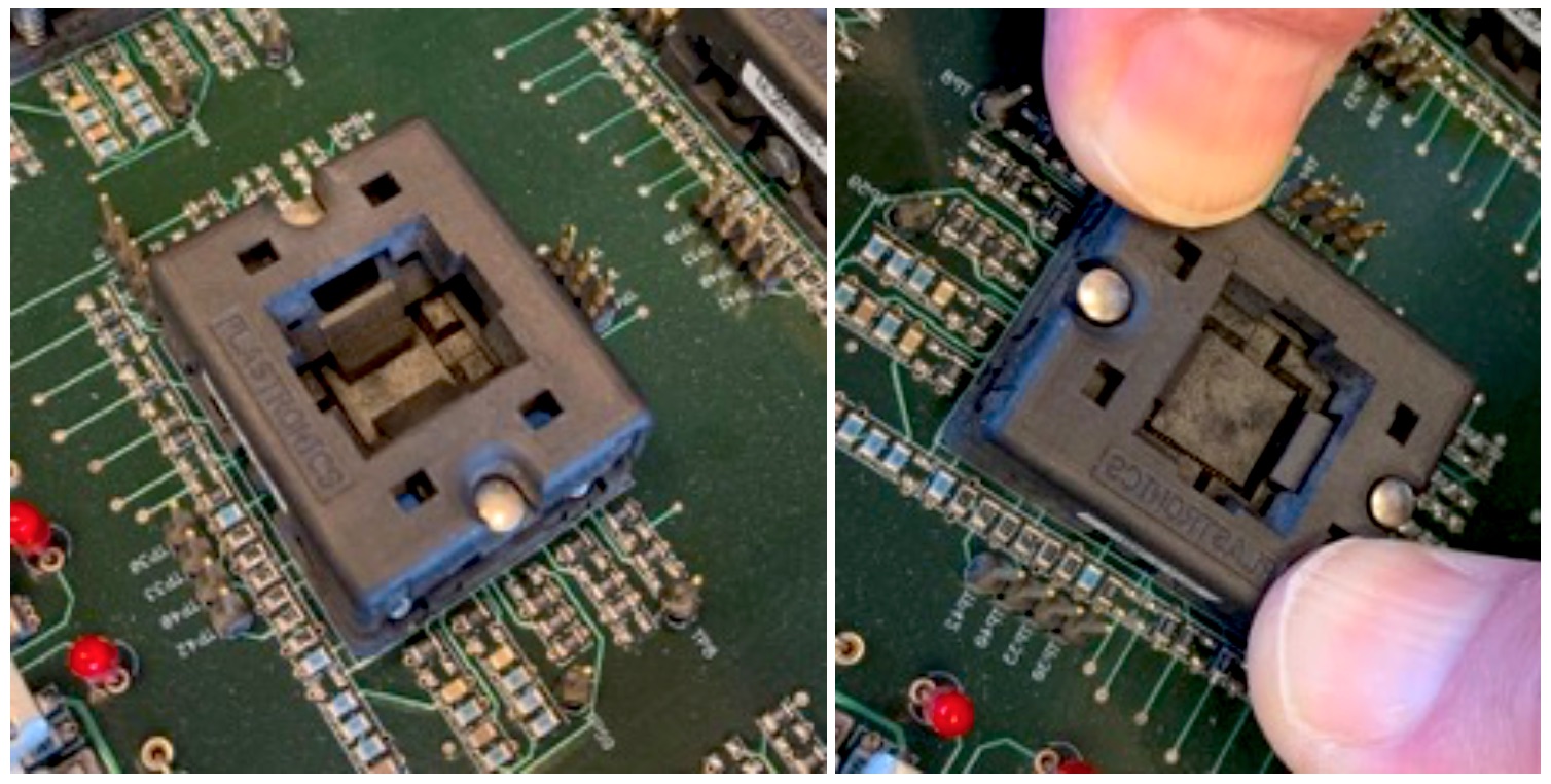
A custom socket by Plastronics. A wide range of socket designs, combined with universal components, can address special testing needs quickly.
Performing burn-in accelerates a component’s lifespan beyond the point of premature failures to weed out defective parts. Components that have passed the burn-in test are highly likely to provide reliable service for the duration of a product’s life.
The process of burn-in testing is undergoing a period of innovation that corresponds with the increase in component and system complexity. As the demands on components increases, the components must be tested to endure greater extremes. To understand how we currently do testing, we need to talk about ovens, sockets, and printed circuit boards (PCBs). We require a test profile for the device under test (DUT), a socket to interface with the DUT and provide signals and power, and an oven to provide the temperature needed to stress the DUT.
Plastronics’ sockets can be used to test at high temperatures, high power, and other factors based on the application needs.
Burn-in ovens provide a stressful test environment by circulating heat around the DUT. The DUT will also generate its own heat within the oven as it processes electrical signals. Ovens used for burn-in testing are evolving to accommodate the increasing temperatures needed to simulate harsh environment operating conditions. Current temperatures range between 125°C (257°F) and 150°C (150°F), with an occasional 180°C (356°F). The automotive industry has been pushing for burn-in temperatures of 200°C (392°F) to 220°C (428°F).
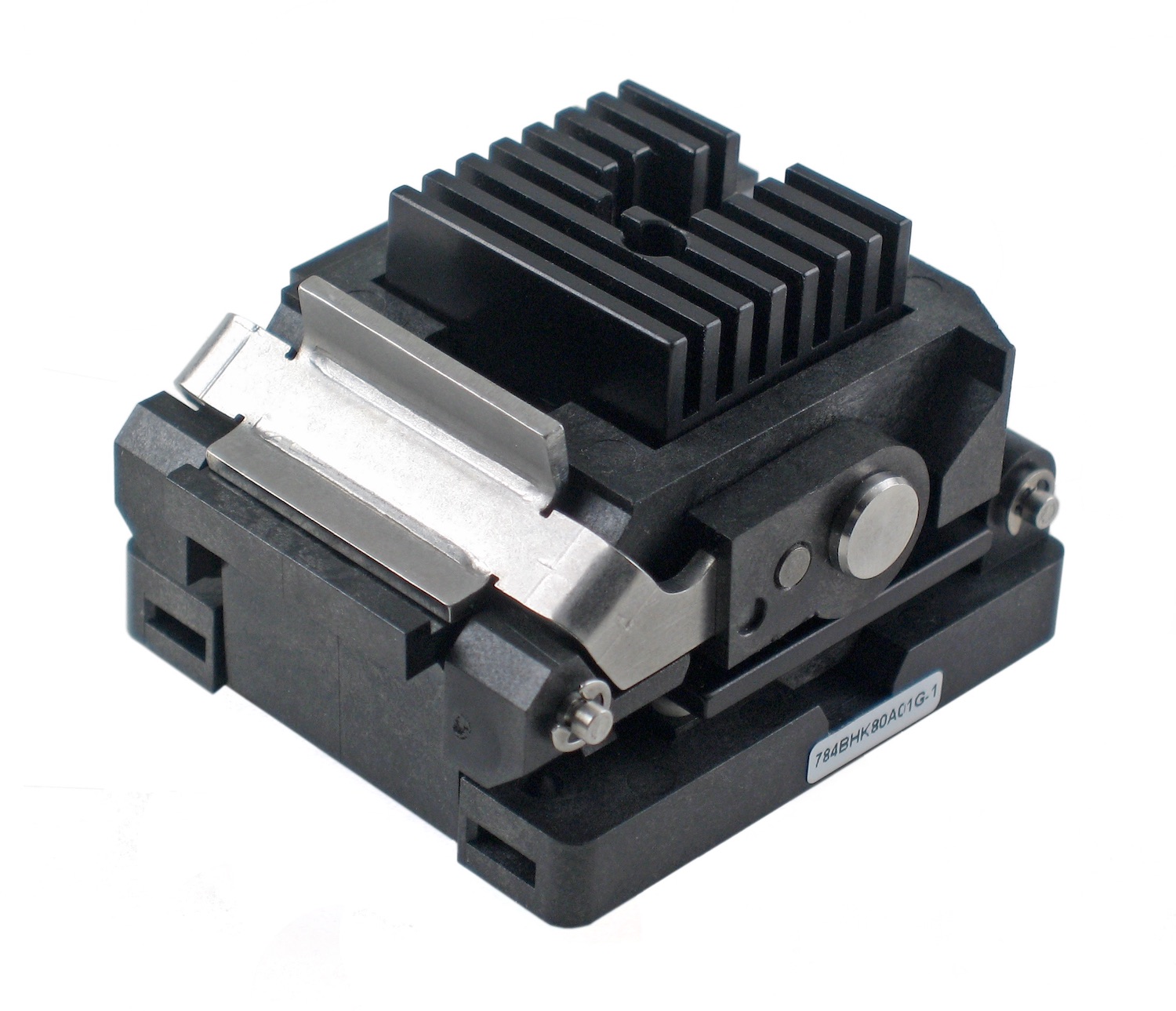
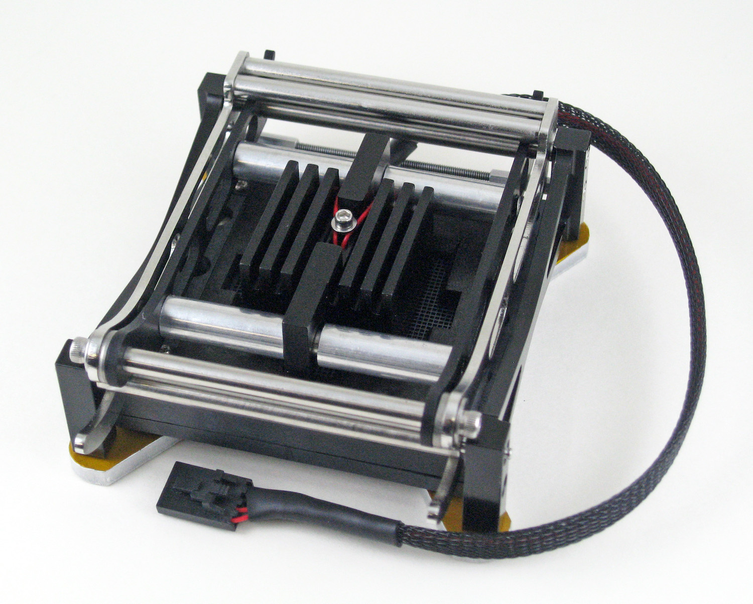
Engineers have lately started reviewing DUT temperatures in ovens more closely. They noticed variations in temperature over the width, depth, and stack height of boards in the oven. They also saw variations in the heat being generated by the individual DUT. To smooth these variations out, the ovens are set at lower temperatures, such as 85°C (185°F) to 100°C (212°F). The sockets are equipped with features such as heat sinks, temperature sensors, fans, and heaters to help individual DUTs achieve a more uniform burn-in temperature. A feedback loop is set up between the heater, fan, and sensor to allow more individual temperature control over each DUT in the oven.
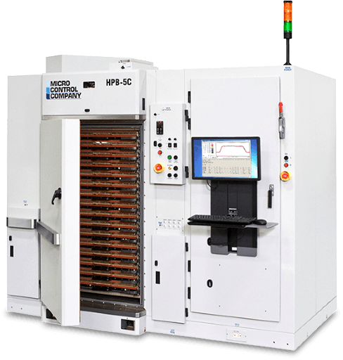
This HPB-5C is one of the many high-power burn-in systems manufactured by Micro Control Company.
Thermal management of individual DUTs is a very “hot” topic right now. Engineers are devising new ways to simulate conditions for an individual DUT in the oven. For example, liquid cooling on individual DUTs within ovens may be used in some cases to test extreme power applications.
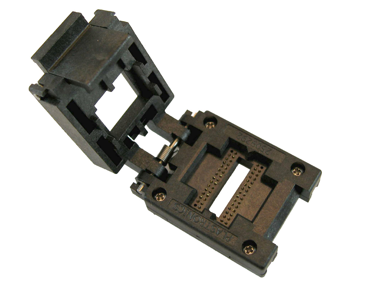
Burn-in sockets are a non-permanent connection from a PCB to a semi-conductor device. The interface at the PCB can either be permanent (soldered) or compression-mounted (semi-permanent). The interface to the semiconductor device (or DUT) is always semi-permanent. This means the DUT can be removed and replaced with another DUT when the test interval has been completed. The burn-in process can then be repeated. In some burn-in processes, the DUT is removed after a few minutes and then the process is repeated with a different DUT. In other cases, the DUT is only removed after thousands of hours of testing. Whether testing is a few minutes or hour, the socket used must work each time another DUT is attached. Sockets typically are made with high temperature plastics, conductive metal contacts, and various springs and hardware. There are basically two types of burn-in sockets, clamshell and open-top. A clamshell socket is self-descriptive. The socket lid delivers force to the DUT to actuate the socket contacts and works in a clamshell fashion. There is usually a hinge pin on one side and a latch at the open end of the lid to hold the lid in place. These types of sockets are typically actuated by hand but can be automatically loaded and actuated using robotic handlers as well. Clamshell sockets come in through-hole mount and compression-mount types, with the latter being a more recent option. Compression-mount types allow the socket to be removed and replaced easily to maintain efficiencies on DUT throughput. Clamshell sockets come in land-grid array (LGA), ball-grid array (BGA), and leaded DUT device formats. Lead pitches in these sockets range from 0.4mm to 1mm. The leading edge is now down to 0.3mm pitch on these devices. These sockets also range in sizes that can accommodate very small DUTs (1mm by 1mm) up to very large devices (70mm x 70mm).
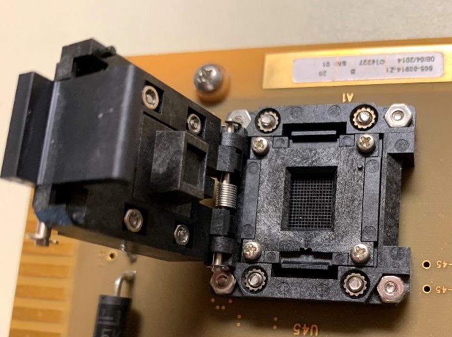
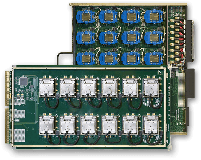
A Plastronics BGA clamshell socket mounted on a PCB. The BGA platform serves package sizes from as small as 6.0mm X 6.0mm to the industry’s largest standard socket for 60.0mm X 60.0mm packages.
An open-top socket is a little less descriptive. In most open-top sockets, you can see a part of the DUT when it is in the actuated position. In a clamshell socket, the DUT is usually covered up by the lid. Unlike a clamshell socket, which is typically actuated by a human or (albeit less frequently) a robotic handler, open-top sockets are often actuated by a machine. The top of the socket is pushed down, releasing spring-loaded latches that hold the DUT in place. In some cases, the latches provide the counterforce to the metal contacts. Open-top sockets are experiencing some changes as well. More and more of them are being manufactured as compression-mount sockets. Compression-mount sockets allow PCBs to be laid out at tighter pitches and enable easy repairs if the DUT or the socket fails.
Before we leave the discussions of sockets, we need to discuss the advent of the stamped probe pin. Probe pins have been around for years. They consist of a screw-machined barrel, one or two plungers, and a spring. There are single-sided moving spring probes as well as dual spring probes, in which both plungers move. Spring probes provide force of a vertical nature and are available with various tip shapes. Spring probes are a great contact mechanism; however, there are a few disadvantages. The assembly process is not easy to automate, so they can be a bit costly. In addition, without automation, producing large quantities can be an issue. These issues have been solved with the invention of stamped spring probes. Stamped spring probes replace the screw-machined barrel with metal stampings that can be produced very quickly in very large quantities. Two stampings are interlocked with a wound spring between them to provide the contact force. The two metal stampings provide the signal path when hooked together.
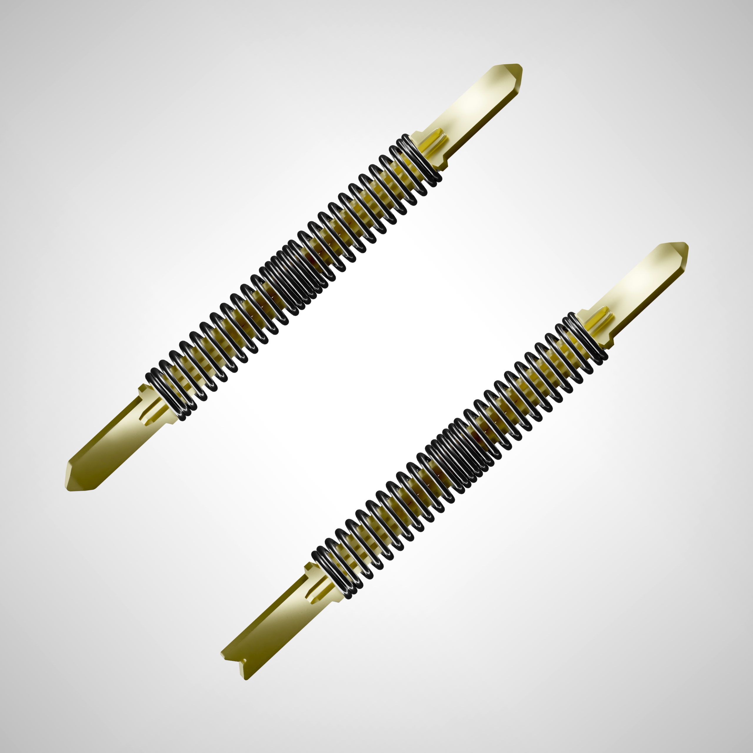
H-Pin stamped spring probes from Plastronics combine the mechanical, electrical, and thermal benefits of spring probes with the high-volume manufacturability and easy use of stamped contacts to achieve high performance at the lowest cost. They support a working range up to 0.70mm, 15GHz with -1.0dB loss, up to 4A and 200°C, and 10,000+ insertions.
These pins allow for almost instant force, as the spring is pre-loaded against the metal stampings. This means that whenever they’re mounted on a PCB, they’re exerting force against the board pads, even when they’re not fully actuated. The pins are assembled and inspected on automatic assembly machines, which increases quality and performance while decreasing cost. In addition, since the metal stampings are attached to a carrier strip, these contacts are automatically loaded into sockets, which reduces socket costs even further.
Typically, burn-in contacts use gold plating with a nickel underplating. A few specialty platings are used, such as nickel boron (NiB); however, these are only available through expensive barrel plating processes. Silver (Ag) plating is now being used as an alternative to gold plating in high-volume, high-cycle applications. Traditionally, expensive vapor deposition was the only method of applying silver. However, recent advances allow silver plating to be applied in a less expensive reel-to-reel plating format that allows it to truly compete on a cost bases with gold plating. Silver is a harder material than gold and has much better conductivity, even greater than copper. This equates to a longer life for the socket contact when applied, less material transfer from the ball or pad to the socket contact, and better contact resistance values. Harder and less material transfer means less contamination of the socket contacts and better resistance means less DUT heating, which means more oven power can be allocated elsewhere.
Printed circuit boards play an important role in burn-in testing. Originally, PCBs were comprised mostly of FR-4 material. Today, in testing applications where high-frequency signals or extreme temperatures are not involved, G10 material is commonly used. PCBs are designed to maximize density while dealing with power management problems. Smaller pitches allow for increased socket density, but power is an issue. With smaller densities, routings require higher board-layer counts, which increases PCB thickness. Today’s standard burn boards range from one to 20 layers, while boards in advanced technologies range from 20 to 30 layers in thickness. As densities increase, trace widths are becoming smaller. Current technologies employ trace widths from 0.008” (0.20mm) to as small as 0.004” (0.10mm), and advanced technology drives this down to 0.003” (0.07mm), or even 0.002” (0.05mm) in extreme cases.
A considerable amount of engineering goes into burn-in, including oven design, test program design, DUT design, socket design, and PCB designs. Many companies farm out pieces of the burn-in process to testing experts, as it is difficult for semiconductor manufacturers to cultivate expertise in all of these fields, particularly during the present period of innovation, which is pushing testing to new levels. Some manufacturers purchase testing ovens for in-house testing and rely on PCB design houses to provide finished boards and sockets for their testing.
Whatever process a company chooses, burn-in testing is an important way to evaluate and ultimately increase reliability. The next time someone asks, “What is burn-in?” you can tell them it’s one of the many ways engineers provide reliability to the semiconductor industry.