Overcoming High-Speed Interconnect Challenges with VNAs
Cloud computing, smart phones, and LTE services are causing a significant increase in network traffic, as well as bottlenecks in high-end services in data centers. Jon Martens and Bob Buxton of Anritsu explain how to overcome high-speed interconnect challenges with vector network analyzers.
Cloud computing, smartphones, and LTE services have caused a significant increase in network traffic, and the instantaneous traffic rates at Internet data centers have reached 1Tbit/s. To support this increased traffic, IT equipment speeds – such as those used in high-end services in data centers – must be increased. Device interconnects are causing transmission bottlenecks in many of these applications. Vector network analyzers can help system designers meet these challenges.
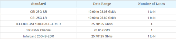
Table 1. 20+ Gbit/s High Speed Standards.
Challenges Facing Signal Integrity Engineers
The move to higher bit rates and the need to ensure compliance with standards raises many issues for signal integrity engineers. These challenges include:
Cost/performance trade-offs
Higher data rates introduce new design challenges such as conductor skin effects and dielectric losses on PC boards, along with the design trade-offs related to choices of vias, stackups, and connector pins. Evaluating a selection of backplane materials and the impact of various structural designs requires accurate measurement in both frequency and time domain. Accurate measurements provide the confidence to make cost/performance trade-off decisions. The aim is to evaluate the impact of interconnects on eye closure. Figure 1 shows an example of backplane impact on the eye pattern.
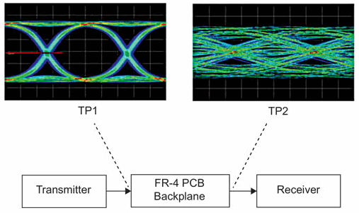
Figure 1 shows an example of a data signal with integrity degradation caused by frequency-dependent loss and group delay effects in the higher frequency bands, resulting from skin effects and dielectric losses on the PC board.
Locating defects
Sometimes problems are caused by vias, stackup issues, and connector pins. However, frequency domain data alone is not enough; it is necessary to transform that data into the time domain in order to locate the position of particular problems. Passive components, as well as near-end and far-end points between daughter boards, must be measured in the frequency and time domains to ensure that the transmission characteristics at each measurement point meet the standards. Using the best resolution capability improves your ability to locate discontinuities, impedance changes, and crosstalk issues. In addition, many of the structures are electrically large and put pressure on the measurement solution’s alias-free range.
Correlation between simulation and measurement
Accurate models help accelerate your design cycle. However, models are only as good as the quality of data fed into them. Poor causality, where outputs can appear to happen in negative time, can be the result of insufficiently high frequency content in the data fed into models. Poor causality results in reduced confidence in simulations, potential convergence problems, and inaccuracies. Conversely, poor low-frequency information leading to DC extrapolation errors also degrades model accuracy and leads to poor agreement with 3D EM simulators.
Fixture de-embedding
There are many situations where it may not be possible to connect directly to the device under test. In this case, it is necessary to de-embed the DUT from the surrounding test fixtures. The opposite is sometimes required: It may be useful to assess a device’s performance when it is amidst other networks. Figure 2 illustrates this.
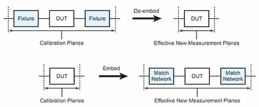
Figure 2: De-embedding can be used to remove test fixture contributions, modeled networks, and other networks described by S-parameters (S2P files) from the measurements. Embedding is the reverse process.
However, many passivity and causality problems are due to poor calibration and de-embedding methods. In addition, high fixture loss may affect the accuracy and repeatability of de-embedding.
Solving Today’s Challenges
Fortunately, the latest vector network analyzer technology can provide a solution to these challenges.
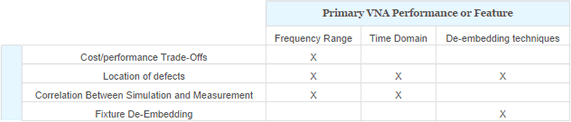
Table 2 shows the relevance of aspects of VNA performance to SI engineer challenges.
Maximizing Available Frequency Range
The lower and the upper frequency limits of an S-parameter characterization of a backplane or other interconnect both have impacts on the quality of the data and any subsequent modeling, but for different reasons. The following will consider each in turn.
The upper frequency range is what usually comes to mind first, and many people perform measurements to the third or fifth harmonic of the NRZ clock frequency. For a 28Gb/s data rate, this means either 42GHz or 70GHz stop frequency for an S-parameter sweep. There is another way to think about the requirement for the upper measurement frequency – from the viewpoint of causality. When S-parameter data is transformed into the time domain for use in further simulation, causality errors can arise; these are essentially where events seem to result in negative time. This can lead to convergence problems in the simulations and inaccuracies in modeling larger-scale subsystems. While massaging the frequency domain data can reduce these problems, there are potential issues related to distorting the actual physical behavior of the device. It is therefore often safer and more accurate to use as wide a frequency range as possible, up to the point where repeatability and related distortions (e.g., the DUT starts radiating efficiently, making the measurement very dependent on the surroundings) obscure the results. The desire for wider frequency range data becomes more compelling as faster and more complex transients are being studied in the higher-level simulations.
The lower frequency bound of the sweep is just as important. Model accuracy generally improves the closer that data is acquired to DC. For example, consider the case where the measured S-parameter data for a backplane is fed into a software model in order to estimate the impact of that backplane on the eye pattern.
Figure 3 shows what the eye pattern estimate will look like where the low frequency data has some error. In this example, it was found that a 0.5dB error distribution at lower frequency (10MHz) on transmission could take an 85% open eye to a fully closed eye. Since mid-band (10GHz) transmission uncertainty may be near 0.1dB depending on setup and calibration – and higher at low frequencies – this eye distortion effect cannot be neglected. Figure 4 shows what the resulting eye pattern will look like if the low frequency measurement data is of good quality and extends down to 70kHz. This prediction correlates very well with the actual eye pattern measured by an oscilloscope, as shown in figure 5.
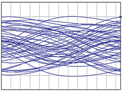 Figure 3: With 0.5 dB insertion loss error at 10MHz |
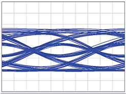 Figure 4: Accurate S-parameter data down to 70kHz reveals an open eye pattern. |
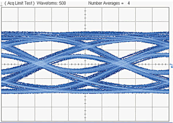
Figure 5: Measured eye pattern
Since the non-transitioning parts of the eye diagram are inherently composed of low-frequency behavior, the sensitivity of the calculation to the low-frequency S-parameter data makes sense. Because the low-frequency insertion losses tend to be small, a large fixed-dB error (which is how VNA uncertainties tend to behave) can be particularly damaging.
Optimizing Time Domain Resolution
The time domain performance of a VNA is critical when trying to locate defects. In general, the wider the frequency sweep, the better the time and, hence, spatial resolution. Figure 6 shows the differences in time domain resolution for three different frequency spans, 40, 50 and 70GHz. Resolution is maximized when low-pass time domain mode is used.
This mode also permits characterization of impedance changes on the backplane. Low-pass mode requires a quasi-harmonically related set of frequencies that start at the lowest frequency possible. A DC term is extrapolated that provides a phase reference, so the true nature of a discontinuity can be evaluated. Hence, the lower the frequency that the sweep can commence, the better the extrapolation of the DC term.
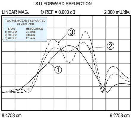
Figure 6: Getting the best time domain resolution requires the most data points, narrowest frequency step size, and widest possible frequency bandwidth.
Using Flexible De-Embedding Techniques
Fixtures and connectors to devices under test come in many forms, and poor de-embedding can lead to both passivity and causality errors. Causality errors were discussed above while passivity errors occur when it appears that a passive device has gain or is otherwise converting energy. The passivity error caused by small de-embedding problems can be subtle, but it can have large effects on follow-on modeling or simulation as suggested by the earlier eye-diagram example. The solution is to have a wide range of techniques available that can handle different situations.
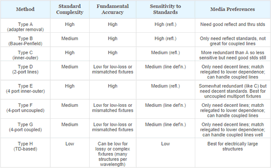
Table 3. De-embedding Methods.
As shown, there are many extraction methods available, and the choice is somewhat context-dependent. For signal integrity applications, the most likely will be type F or G. Higher data rates require accurate measurements to make confident performance/cost decisions. Measurement tools must help shorten design times and ensure stable signal integrity in mass production. Vector network analyzers play a key role in helping the signal integrity engineer meet the challenges of increasing data rates, make appropriate cost/performance trade-offs, achieve correlation between simulations and measurement, and extract the effect of fixtures. When selecting a VNA, the user should look at characteristics such as upper and lower frequency limits, performance in time domain, and a wide selection of advanced calibration and de-embedding techniques.
[hr]
To see the original version of this white paper, click here.
Jon Martens and Bob Buxton work for Anritsu.