Managing Next-Generation High-Speed Signals
The physics associated with electronic signaling may point to the need for a more holistic system approach to higher performance.
At the beginning of the electronics era, the biggest challenge circuit engineers faced was designing low-resistance links between components. Very-early electronic systems often used discrete wire to make these connections, a process that was labor-intensive and prone to wiring errors.
Organizing components mounted on printed circuit board material began by soldering component leads between boards that featured etched copper traces to create conductive paths between components. These “cordwood” modules were more manufacturable and offered a degree of modularity.
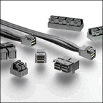
Over time, printed circuit boards have evolved into highly sophisticated multilayer motherboards, daughtercards, and backplanes that are designed according to tight mechanical and electrical specifications. Components attached to these boards are often wave-soldered or surface-mounted using reflow soldering techniques. PCB board interconnect technology evolved to support thousands of links at ever-higher packaging density. Connectors adapted to these new board configurations with compliant press-fit solderless termination as well as pin grid, land grid, and ball grid array technology.
Circuit designers today are facing a daunting set of challenges in the management of high-speed signals that include requirements for tight impedance control as well as limits on crosstalk, skew, latency, electromagnetic interference, and attenuation. As data rates continue to rise, the potential for signal distortion and attenuation increase. Loss and distortion also increase as links become longer. Ground planes must be carefully designed to ensure proper coupling. Wide PCB traces offer better high-speed performance but reduce circuit density. Narrow traces exhibit greater signal loss and are more difficult to manufacture. Inaccurately aligned layers in a large backplane can result in costly waste. All of these factors must be carefully considered during the high-speed PCB circuit design and layout process. Simulation of circuit performance has become standard procedure.
As signal speeds increase, the characteristics of the PCB laminate material have greater influence on the signal integrity of the circuit path. Standard FR-4 laminates are being upgraded to enhanced versions that offer a range of dielectric constants, lower dissipation factors, and mechanical properties that feature greater uniformity. Even the type of glass weave and degree of moisture absorption become design considerations. High-performance laminates feature excellent high-speed characteristics but at a significantly higher price.
As a result of these and other factors, as data rates increase, the effective design length of copper conductors on a PCB as well as in cables is becoming shorter. The electronics industry has been actively developing solutions to address this problem.
Integration of many functions into the semiconductor chip itself has completely eliminated many external links to other components. Physically packaging the system to reduce the size of the product not only minimizes signal 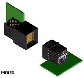 lengths but offers advantages to the consumer in terms of greater product function and mobility. Microservers, for example, are often designed around system-on-a-chip devices that integrate the CPU, memory, and I/O on a single chip to achieve much higher system packaging density. Many microservers can be packed in clusters to save space in a data center and reduce interconnect lengths between servers.
Traditional backplane packaging is being supplemented with mid-plane orthogonal and direct orthogonal architecture that can dramatically reduce channel circuit path lengths between daughtercards.
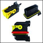
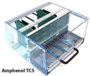 As system complexity and circuit density continues to increase, designers have begun looking at the possibility of replacing etched copper traces on the backplane with shielded differential cables. Impedance control and attenuation as well as signal isolation can be more effectively managed in shielded cable. High-speed signals are passed through the backplane directly to short cable assemblies that deliver signals among daughtercards. A simplified backplane continues to distribute low-speed signals and power. Several leading high-speed backplane connector manufacturers have introduced cable backplane systems that utilize pluggable discrete or ribbonized shielded cables. Cable backplanes have seen relatively few volume implementations to date, primarily due to higher costs, as well as issues relating to cable management.
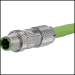
The maximum effective length of a standard I/O interconnect is often defined in the specification or learned from experience. Active optical cables can be used to extend this length by converting electronic signals to optical at one end and reconverting them at the far end. The majority of the signal path is in optical fiber, which exhibits much lower attenuation and distortion than an equivalent length of traditional copper cable.
 Even the relatively short internal links that run from processors, ASICS, and SERDES devices are being looked at to improve performance. One solution is the use of mid-board optical transceivers. These devices can be located adjacent to a component to take the high-speed signal off the PCB entirely, convert it to an optical signal, and deliver it directly to the backplane interface or I/O port. The PCB laminate can remain a low-cost material as it conveys only low-speed signals and power. PCB layout is simplified, reducing the design cycle and risk associated with a new design.
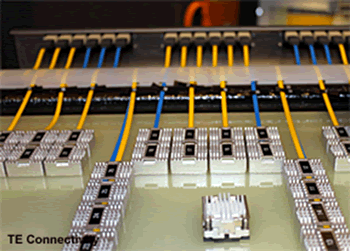
The physics associated with electronic signaling may point to the need for a more holistic system approach to higher performance. A recent initiative is the announcement of the Intel Omni-Path Architecture, a new high-performance fabric designed to support next-generation supercomputer switches and servers. A part of this concept calls for replacing traditional copper traces on PCBs with shielded differential cables in select high-speed, point-to-point, as well as backplane and I/O port, circuits. Both copper and fiber links will be utilized. Once again, high-speed signals are taken off the PCB to improve signal integrity and potentially reduce cost. Details on the specific interconnect hardware to be utilized in this new fabric are being carefully managed by Intel, but industry-leading connector manufacturers including FCI, Molex, and TE Connectivity are known to be working with Intel on these interfaces.
The recently announced Aurora supercomputer that will be installed at the Argonne National Laboratory will be built using Omni-Path Architecture. This machine will feature over 50,000 nodes and multi-million cores while consuming 13 megawatts of power. This new architecture is the next step in the path to Exascale computing, but over time may also demonstrate a migration path to higher performance of entirely new classes of electronic computing devices that may eventually appear in commercial and consumer products.
Stay tuned as more details are revealed.


- XPO, Addressing the I/O Panel Bottleneck - June 30, 2026
- Agentic and Neuromorphic Computers Enable the Future of Digital Computing - May 26, 2026
- OFC 2026: High-Speed Networking in the AI Era - April 7, 2026