PCB Connector Termination Evolution Continues
PCB Connector Termination Evolution Continues
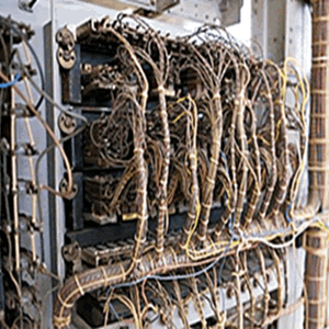 The concept of creating a custom pattern of conductive copper circuits on the surface of a ridged substrate forever changed the way electronic devices were packaged. Early systems were a maze of discrete wires that required massive amounts of hand assembly and were prone to wiring errors and cold solder joints.
The printed circuit board enabled designers to mechanically mount and electrically connect many discrete components mounted on a manufacturable and reproducible platform.
Highly reliable wiring patterns, created using photo-etching processes, could be quickly changed with minimal tooling. Once designed and verified, tight process control enabled production of thousands of identical boards, essentially eliminating the potential for human error.
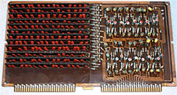 PCBs continued to evolve in size, complexity, and performance. Single-sided boards with components on the top and traces on the underside morphed into multilayer boards consisting of multiple embedded copper layers laminated into a single assembly. These assemblies provide literally thousands of interconnecting links among devices mounted on one or both surfaces. Plated thru-hole technology provides the ability to connect selected layers within the board, while advances in the board dielectric material have enabled transmission of multigigabit signals. Shrinking trace dimensions and automated layout software enable precise impedance control and allow accurate prediction of crosstalk in high-speed circuits.
Industry adoption of printed circuit boards introduced a challenge in reliably terminating discrete wire and connectors to the PCB. Unlike a crimp produced by a precision tool, the quality of a soldered joint is highly dependent on the skill of the operator. A wire can be poked into a hole surrounded by a copper pad and hand-soldered, but the wire can easily be pulled out prior to soldering or moved before the solder joint has cooled. Any wire stub extending below the board required a separate cut-off operation. Several connector manufacturers developed tiny contacts that were crimped on the stripped wire and clipped into the hole to ensure retention prior to soldering.
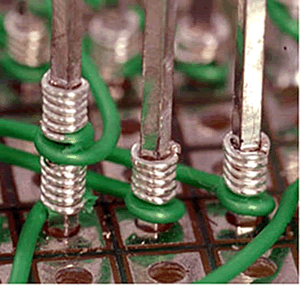 Another approach, wire wrap, was extensively used in commercial computing equipment in the 1960s. A square metal post was staked into holes on the PCB. Using a special tool, a stripped wire was tightly wrapped around the post several times. The sharp corners on the post dug into the silver-plated wire and created multiple gas-tight points of contact. A wire-wrap termination exhibited lower contact resistance than a typical solder joint and was more repeatable. Wire-wrap terminations were limited to solid conductor wires, prompting AMP to introduce its Termi-Point clip system that could clamp a stranded wire to a side of the post. A wide variety of backplane and other standard connectors were adapted to accept wire-wrap and Termi-Point termination. Each of these methods produced a semi-permanent connection to the board, but a separable connection makes more sense in many applications.
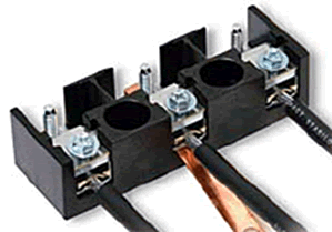 Discrete wires that require connection to a PCB in the field, such as applications in industrial control, can be terminated using terminal blocks soldered to the PCB.
Attaching a connector to a PCB introduced a whole new set of challenges to the designer. Initially, connectors were fitted with short solder posts and hand soldered from the underside of the board. Soldering hundreds of individual connections proved time-consuming and a potential existed for poor quality solder joints.
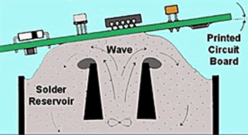 Mass soldering techniques, such as wave solder, where the underside of the PCB is preheated, fluxed, and passed over a wave of molten solder, solved the problem. The process can be precisely controlled to match the requirements of individual boards and result in uniform and reliable solder joints. Exposing the connector to elevated soldering temperatures required the use of plastic materials that could withstand this heat without deformation.
Large, multilayer backplanes posed problems in ensuring adequate solder reflow temperatures when attaching backplane connectors. Many layers of embedded copper traces can act as an effective heat sink, potentially resulting in cold solder joints. Raising the soldering temperatures can damage these expensive boards.
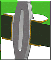 The solution was the development of compliant pin technology, where a portion of the connector termination area has been formed into a spring beam. When pressed into a plated thru-hole, the beam compresses against the walls of the plated hole and creates a gas-tight connection. This process avoids potential damage from the heat of a soldering process and connectors can be mass-applied by simply pressing them into the backplane. A variety of compressive contact designs were introduced over the years, with variations of the “eye of the needle” becoming widely adopted. The advantages of the press-fit connection were quickly recognized, but questions about potential damage to the plated thru-barrel and long-term reliability of this solderless connection delayed general adoption for many years. Compliant pin termination has now been fully accepted and is available on a wide variety of connector types, including power and signal interfaces.
Drilling thousands of thru-holes in a PCB is a costly and time-consuming process. Elimination of the thru-hole is attractive. Adoption of surface-mounted components reduced the number of drilled holes and created the need to adapt connectors for compatibility with surface-mount reflow soldering processes. A wide variety of surface-mount footprint designs have entered the market and are designed to compensate for PCB warp, coplanarity, and thermal expansion.
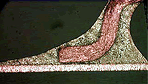 Many surface-mounted connectors sport mechanical hold-down features that ensure that the surface-mount legs are in physical contact with the solder pad to create a proper solder fillet.
With the introduction of RoHS, tin/lead solders were replaced with pure tin, which require higher reflow temperatures. In many cases, plastic connector materials were upgraded to liquid crystal polymers capable of resisting deformation at elevated temperatures.
Standard thru-hole connectors that have been adapted for surface-mount compatibility continue to be popular. In this case, rather than applying solder paste to surface pads, it is screened into the hole. The connector is inserted through the paste and then reflowed along with all other components on the board.
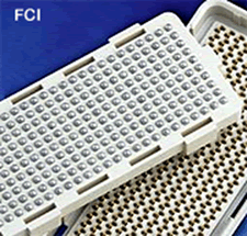 A variation of surface-mount termination is the ball grid-attach (BGA) method, where balls or columns of solder are pre-applied to the bottom of a connector. This approach eliminates the need for applying solder paste to the surface-mount pad when reflowed in a hot air oven. Low-profile, high-density interconnects, such as mezzanine connectors, benefit from the advantages of BGA attachment.
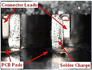 Several connector suppliers, including Molex and Samtec, have taken surface-mount technology one step further by attaching a carefully controlled solder slug directly to the PCB tail of the surface-mount connector. This approach results in an ideal solder fillet that is mechanically stronger, easier to inspect, and more forgiving of board warp.
A huge variety of connector types are now available in both thru-hole and surface-mount termination. One major exception has been large backplane connectors. Designers remain concerned about surface-mount solder joint fracture due to thermal expansion as well as the mechanical stress generated when daughtercards are mated with the backplane connector. Surface-mounted high-speed backplane connectors that replace large plated thru-holes with very small vias may offer some improvement in signal integrity, but the industry is not yet ready to adopt this technology.
Several categories of connectors are terminated to the PCB using compressive spring contacts mating with gold- or tin-plated pads on the board. They provide a solderless low-profile connection that is easy to assemble. The connector can be mechanically screwed down to the board, which establishes a high-pressure interface. Connectors may make compressive contact to the PCB or act as an interposer with contacts on both sides for parallel board-to-board or board-to-flex circuit links.
Yamaichi, for example, offers AdvancedTCA and MicroTCA connectors that are terminated to the PCB using compressive contact technology. Molex, Delphi, Cinch, and others offer connectors using compressive attachment.
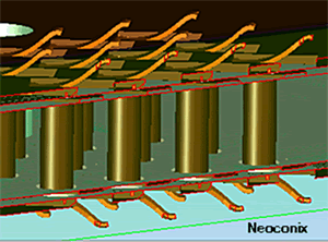 Several attempts to adapt large backplane connectors with compressive termination have proven unsuccessful. These connectors are typically longer and may incorporate hundreds of contacts on small centerlines. The pressure they exert on the backplane may warp the board, thus requiring the use of large stiffening bars. Additional questions have been raised about ensuring proper assembly both initially and in the field.
The process of attaching wire and connectors to the printed circuit board has continued to evolve over the years to satisfy industry demand for reliable and manufacturable interconnects. Recognizing the critical role that these connections play in the reliability of the product, manufacturers have slowly adopted new methods of connector termination only after years of process verification. Designers now have multiple options that feature cost-effective manufacturability as well as a high degree of long-term reliability.
- Optics Outpace Copper at OFC 2024 - April 16, 2024
- Digital Lighting Enhances your Theatrical Experience - March 5, 2024
- DesignCon 2024 in Review - February 13, 2024

