Battle on the I/O Panel
Semiconductor suppliers and data center managers keep increasing the volumes of data flowing through cables. That’s putting a lot of pressure on connector makers who have to meet these demands while reducing size. Optics may provide a solution.
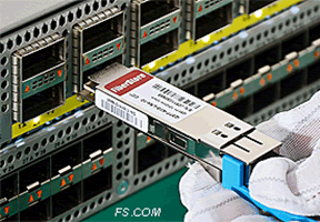 The semiconductor industry has done an incredible job of increasing data rates and memory capacity, two key factors that have enabled the industry to continue advancing at breakneck speed. We are now reaching a point where computing power may be throttled by the inability of the system to transfer data in and out at a comparable rate. The I/O panel of the typical server or switch has become a focal point of efforts to move terabits of data in and out of a panel that measures only 1.7” by 18”. System designers labor to increase effective signal transfer per square centimeter.
In today’s high-speed electronic systems, increasing data throughput can be accomplished in several ways. Serial data rates have increased dramatically. But in copper circuits, that raises signal integrity concerns such as crosstalk, attenuation, return loss, skew, jitter and EMI.
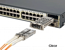 As signal rates increase, the practical length of a copper circuit typically becomes shorter for a given material, limiting designer flexibility. One approach is to aggregate data from several parallel channels that run at lower speeds. This lets engineers design in their comfort zone, but multiple differential channels require more pins in the I/O connector, making it physically larger.
Another option is to use higher performance PCB materials or utilize twinax cables inside the box, but this likely adds significant cost. A third solution is to transfer more information per signal clock cycle. That is what PAM4 signaling can do, but it can add complexity and cost while increasing power consumption. Finally optical interfaces offer exceptional signal density, but for most short runs is often cost prohibitive. The electro-optical conversion process required at both ends also draws more power and generates unwanted heat.
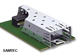 The most practical solution today revolves around a continually evolving series of pluggable interfaces that offer design flexibility, as well as high speed and signal density. A pluggable copper or optical transceiver module is mated with a high-speed PCB connector located at the rear of an EMI shielding cage assembly.
The original concept for a pluggable I/O interface goes back to 1995, when the Gigabit Interface Converter (GBIC) was developed. This hot-swappable module and socket enabled system designers and architects to select high-speed copper or fiber optic interfaces to address specific application requirements.
The concepts of this system spawned a series of small form factor pluggable connectors that offer greater channel speed and signal density. Managed by a Multi-Source Agreement (MSA), the SFP specification has been upgraded over the years from one Gb/s to SFP+ capable of sixteen Gb/s/channel in the same module envelope. SFP28 is the latest iteration with data rates to 28 Gb/s/channel.
QSFP (quad SFP), embedded four 10 Gb/ channel links in a single connector shell. The most recent QSFP28 upgrade enables the ability to support 100 Gb Ethernet and Infiniband EDR via 4 X 25 GB channels. System designers can choose direct copper cables, active optical or fiber optic I/O options which can be altered in the field as requirements change.
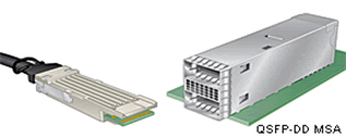 Additional pluggable interfaces continue to be proposed or are entering the market. The QSFP double-density MSA is defining an 8 lane by 25 Gb interface to address 200 Gb applications.
CXP connectors deliver 10 Gb/s over 12 fiber or copper lanes for an aggregate of 120 Gb/s. CDFP 2.0 is designed to support data rates of 25 Gb/s over each of 16 lanes of optical fiber for an aggregate of 400 Gb/s.
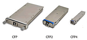 CFP 2/4 has been specifically optimized for longer distance optical links. Each progression in this series has reduced the physical size, power consumption and PCB pin count of the interface.
The race to higher speed and panel density continues.
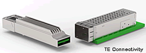 TE Connectivity introduced the Micro QSFP, which also addresses the thermal issues associated with squeezing more electronics into smaller spaces. Thermal fins on the pluggable module and a vented PCB cage assembly efficiently transfer heat out of the module. Packaged in an envelope slightly larger than the standard SFP connector, the Micro QSFP can be configured with one, two or four channels to support up to 100 Gb/s applications. Up to 72 ports can be mounted on a 1U faceplate delivering a total of 7.2 Terabits per second.
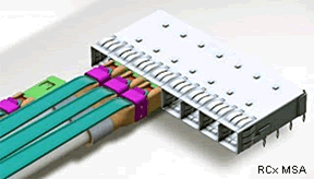 Amphenol FCI and JAE have joined a new MSA and announced development of the RCx, a 25 Gb/s per lane passive I/O connector system that specifically focuses on low cost. The RCx interface is designed specifically for direct attach copper cables in relatively short lengths of up to three meters without forward error correction. It is intermateable with existing SFP and QSFP PCB cage assemblies. RCx is optimized to accommodate more than 128 25G lanes on a 1 U faceplate.
Adding to the mix of requirements is customer demand for mechanically and electrically identical interfaces from multiple sources. Most new connectors in the high-speed I/O arena are supported by MSAs that often include both connector manufacturers and OEM’s. Molex and TE Connectivity recently announced their participation in a Dual Source Alliance (DSA) that will focus on next generation high-speed backplane and I/O connectors with up-front competitive second sources.
High performance, datacenter-focused connectors have become a highly competitive market that will likely remain a fierce battleground among suppliers. As 100 Gb links evolve to 400 Gb and beyond, optics will likely play a larger role in the I/O panel arena resulting in a continuing evolution of these interfaces. Access to the necessary technical expertise and a willingness to participate in collaborative product development programs will insure that I/O connectors will avoid becoming a data bottleneck.
Recently posted:
[related_posts limit=”10″]
- OFC 2026: High-Speed Networking in the AI Era - April 7, 2026
- DesignCon 2026 - March 17, 2026
- Breaking Through the AI Power Wall - January 20, 2026


